Availability
Published
Product Code
APE-2007-801
Product Item Code
INT-SRH4U
Device Manufacturer
Intel
Device Type
Applications Processor
Subscription
Advanced Packaging
Channel
Advanced Packaging - Process
Intel SRH4U Foveros 3D PoP Technology Advanced Packaging Essentials
This is an Advanced Packaging Essentials of the Intel SRH4U Forevos3D package-on-package (PoP) technology. The Intel SRH4U processor was found in the Samsung Galaxy Book S tablet.
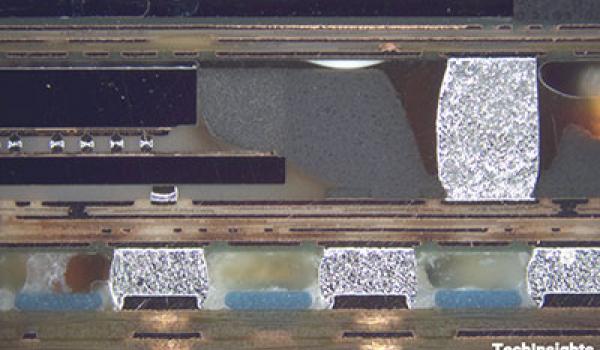
The complete APE deliverable includes a concise analyst’s summary of critical device metrics, scanning electron microscopy (SEM) based energy dispersiveX-ray spectroscopy (SEM-EDS) of package materials, and salient features supported by the following images:
The complete APE deliverable includes a concise analyst’s summary of critical device metrics, scanning electron microscopy (SEM) based energy dispersiveX-ray spectroscopy (SEM-EDS) of package materials, and salient features supported by the following images:
- Downstream product teardown
- Package photographs and X-rays
- Die photographs
- Optical planar view images of selected PWB metal layers
- SEM, TEM, and optical cross section of the general package structure, metals, dielectric materials, die, TSV and package interconnect structure
![]()
The Authoritative Information Platform to the Semiconductor Industry.
