Advanced Packaging
Enhance Performance & Efficiency with TechInsights
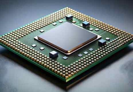
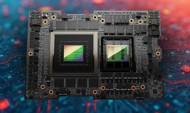
Advanced Packaging is transforming the semiconductor industry by rethinking how integrated circuits (ICs) are connected in electronic systems. This innovative approach enhances performance, speeds up multi-chip processors, and boosts interconnect density while improving power efficiency. By integrating chiplets and sub-components, Advanced Packaging enables more flexible, scalable, and energy-efficient solutions. It goes beyond technology, offering a strategic tool to achieve key goals in power, performance, area, cost (PPAC), value, and sustainability.
1.5M+
Reports
100K+
Chip Teardowns
650+
Global Customers
30+
Years of Experience
Driving Innovation
By delivering in-depth insights into the latest technologies and market dynamics, Advanced Packaging empowers enterprises to innovate confidently, ensuring they remain at the forefront of the semiconductor industry.
Key Features & Industry Insights
- Market Dynamics and Technical Insights: Gain a privileged view of the rapidly evolving Advanced Packaging landscape, supported by deep technical analysis of commercialized technologies.
- Strategic Roadmaps: Utilize technical analysis insights to understand technology insertion timelines and stay ahead of industry trends.
- Technical Roadmap and Interconnect Scaling: Benefit from our analysts' detailed comparisons, dimensional analyses, and reviews of enabling technologies to guide your innovation strategies.
Predicting Future Node Requirements with TechInsights' Compute Analysis
Gain a competitive edge with TechInsights' Compute, leveraging in-depth analysis to predict future node requirements and optimize technology decisions.
Optimizing Compute Floorplans and Technology Selection for Faster Development
Optimize floorplans and technology selection with TechInsights’ Compute analysis. Ensure product alignment, accelerate development, and enhance design efficiency.
Using TechInsights Compute Offering to Mitigate Core Design Risk
Discover how one of the world’s leading CPU providers leveraged TechInsights’ Compute offering to enhance their semiconductor analysis and mitigate core design risk.
Targeting Markets
Our advanced demand models and market forecasts enable enterprises to effectively target their offerings, ensuring they align with market needs and capitalize on emerging opportunities.
Market Understanding and Expertise
Our deep market knowledge and analysts' domain expertise will build demand profiles that drive accurate bottom-up forecasts segmented by interconnect methods, substrate types, and more.
Demand Modeling
Our advanced models forecast design starts, revenue, and unit shipments, providing crucial insights for wafer fab equipment (WFE) and related markets.
Strategic Market Inputs
Our comprehensive market analysis directly informs our technical analysis, guiding product sourcing and target selection to ensure alignment with market needs.
Unlock the Power of Advanced Packaging
Advanced Packaging from TechInsights is designed to help your business drive innovation and effectively target markets.
Frequently Asked Questions
Advanced Packaging is a semiconductor technology that enhances the way integrated circuits (ICs) are connected within electronic systems. It improves performance, power efficiency, and interconnect density while enabling miniaturization and chiplet-based architectures.
Unlike traditional packaging, which primarily focuses on housing and protecting ICs, Advanced Packaging integrates high-density interconnects, heterogeneous integration, and chiplet architectures to optimize power, performance, and space efficiency.
Advanced Packaging provides several advantages, including:
- Miniaturization – Enables compact designs for space-constrained applications.
- Higher Performance – Enhances speed and efficiency in multi-chip processors.
- Increased Interconnect Density – Supports more connections within a smaller footprint.
- Power Efficiency – Reduces energy consumption for sustainable applications.
- Scalability – Allows for modular, flexible designs through chiplet integration.
Advanced Packaging is essential for industries requiring high-performance, energy-efficient solutions, including AI, data centers, mobile devices, automotive, and IoT.
It optimizes Power, Performance, Area, and Cost (PPAC) by improving chip efficiency, enabling compact form factors, reducing energy consumption, and lowering overall manufacturing costs.
TechInsights provides in-depth analysis, insights, and reports on Advanced Packaging trends, technologies, and competitive landscapes to help businesses drive innovation and make informed strategic decisions.
Contact us today to explore how Advanced Packaging can benefit your business. Request a Demo to see our solutions in action.
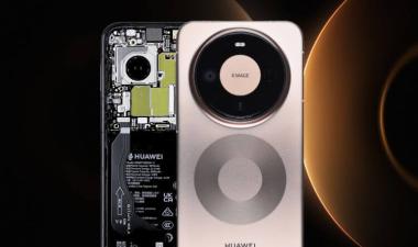
Huawei Mate 80 Pro Max Teardown Confirms Kirin 9030 Pro on SMIC N+3
TechInsights’ teardown of the Huawei Mate 80 Pro Max confirms the Kirin 9030 Pro on SMIC’s N+3 process and reveals major upgrades in display, cameras, and connectivity.
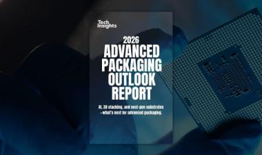
2026 Advanced Packaging Outlook Report
Discover the five expectations defining advanced packaging in 2026, including CPO adoption, HBM4 demand, panel and glass scaling, 3D thermal challenges, and chiplets for mobile.
Trump Approves H200 Exports: Impact on NVIDIA, TSMC & HBM
Trump’s approval of H200 exports to China could reshape GPU, packaging, and HBM markets. TechInsights analyzes supply constraints, pricing, and $40–50B demand.
![]()
The Authoritative Information Platform to the Semiconductor Industry.
