Availability
Published
Product Code
ACE-1810-803
Product Item Code
SAM-SM-R810
Device Manufacturer
Samsung
Device Type
Smartwatch
Subscription
Advanced Packaging
Channel
Advanced Packaging - Process
Samsung Exynos 9110 Samsung Fan-Out Panel Level Packaging - Advanced Packaging Essentials
This is an Advanced CMOS Essentials (APE) Summary document of the fan-out panel level package (FO-PLP) built using Samsung’s next generation of semiconductor packaging technology. Concise analyst’s summary of critical device metrics, scanning electron microscopy based energy dispersive X-ray spectroscopy (SEM-EDS) of package materials, and salient features supported by the following images:
- Downstream product teardown
- Package photographs and X-rays
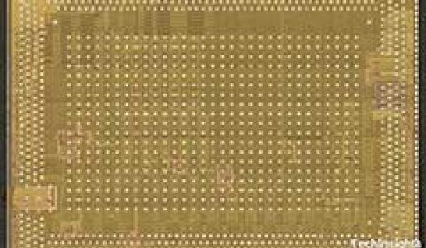
- Die photographs
- Optical planar view images of the redistribution layers (RDLs) and the embedded printed wiring board (PWB)
- SEM and optical cross section of the general package structure, and targeted SEM cross section of the metals, dielectric materials, RDL interconnect, embedded PWB and PoP interconnect
![]()
The Authoritative Information Platform to the Semiconductor Industry.
