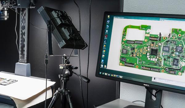
This is an Advanced Packaging Essentials of the GaN Systems GS66508T and GS66508B 650 V E-mode GaN transistor embedded die package technology. Each of the GS66508T and GS66508B components is an enhancement mode GaN-on-silicon power transistor and uses embedded die package technology. The power transistor die is fully embedded in a two-layer printed wiring board (PWB).
- Downstream product teardown
- Package photographs and X-rays
- Die photographs
- Optical planar view images of the redistribution layers (RDLs)
- SEM and optical cross section of the general package structure, and targeted SEM cross section of the metals, dielectric materials, RDL interconnect, and vias


