Availability
Published
Product Code
APE-2001-801
Product Item Code
QUA-QET5100M
Device Manufacturer
Qualcomm
Device Type
Envelope Tracking Power Supply
Subscription
Advanced Packaging
Channel
Advanced Packaging - Process
Qualcomm QET5100M Advanced Packaging Essentials
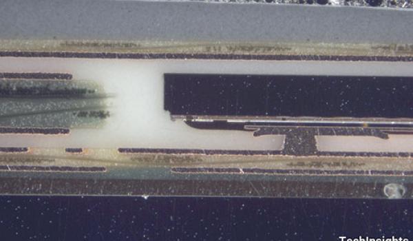
This is an Advanced Packaging Essentials on the Qualcomm QET5100M Envelope Tracker Module Embedded Die Technology. The envelop tracker IC is embedded in a six layer PWB organic substrate. Passive components are surface mounted on the PWB substrate, and overmolded. Metalized overmold provides EMI shielding.
- Downstream product teardown
- Package photographs and X-rays
- Die photographs
- Optical planar view images of the redistribution layers (RDLs)
- SEM and optical cross section of the general package structure, and targeted SEM cross section of the metals, dielectric materials, RDL interconnect, and vias
![]()
The Authoritative Information Platform to the Semiconductor Industry.
