A Tale of Three Phone Chips: Eco Edition
Author: Lara Chamness
Did you know that emissions from the manufacture of the processor in your mobile phone could easily be the equivalent of driving over seven miles in a gasoline-powered car? Despite consumer interest in sustainability, phone reviews often overlook carbon emissions. So, let’s lift the screens, so to speak, and perform a preliminary emissions analysis of three processors used in today’s flagship phones from Apple, Huawei and Samsung. While process node, fab location, and abatement efficiency have a strong impact on the carbon intensity of semiconductors, our review found die size has a more significant impact on the processors we evaluated.
It is no secret semiconductor manufacturing is energy intensive and uses a variety of high Global Warming Potential (GWP) gases to create intricate circuitry patterns on silicon wafers. Yet, despite the growing importance of sustainability considerations to consumers, reviews of mobile phones typically focus on cameras, battery life, cellular connectivity, and overall performance, rather than carbon emissions associated with these mini-super computers. That’s unfortunate, as not all semiconductor manufacturing processes are created equal when it comes to their impact on the environment. Greenhouse gas (GHG) emissions from semiconductor manufacturing can vary greatly depending on the technology process node being manufactured and the location of the wafer fabrication (fab) facility.
Whether you are an Apple iPhone aficionado, a Samsung Galaxy supporter, or a Huawei Mate mega fan, all mobile phones have a sizeable lifecycle carbon emissions footprint, of which roughly 80% can come from manufacturing. To gain insight into emissions associated with the manufacture of mobile phones, three processors used by Apple, Huawei, and Samsung (Table 1) in their most advanced phones were evaluated. We have deep-dive teardown analysis available for all three handsets in our technical analysis content, also linked in the table.
| Phone | Processor | Foundry Partner | Fab Location | Fab Abatement | Process Node | Die Area (mm2) |
|---|---|---|---|---|---|---|
| Apple iPhone 15 Pro Max | A17 | TSMC | Taiwan | 90% | 3nm | 112.8 |
| Huawei Mate 60 Pro+ | Kirin 9000s | SMIC | China | 60% | 7nm+2 | 108.9 |
| Samsung Galaxy S24 Ultra | Qualcomm SM8650-AB | TSMC | Taiwan | 90% | N4P | 137.5 |
Table 1. Smartphone models analyzed. TechInsights, 2024.
Die size significantly impacts semiconductor carbon emissions; as the die size increases, yields go down, resulting in an increase of emissions per good die. Reviewing Scope 1 (direct greenhouse gas emissions occurring from sources that are controlled or owned by the fab) and Scope 2 (indirect emissions associated with the purchase of electricity) emissions per wafer in terms of carbon dioxide equivalents (CO2e)1, the Qualcomm SM8650-AB has the lowest emissions per wafer, followed by the A17 and Kirin 9000s (Figure 1). When emissions per die are evaluated, the trend reverses; the largest processor, the Qualcomm SM8650-AB has the highest emissions per die, while the smallest processor, the Kirin 9000s, has the lowest total emissions.
Figure 1. Comparison of Processor Manufacturing Emissions by Die and Wafer. Source: TechInsights’ Semiconductor Manufacturing Carbon Model, 2024.
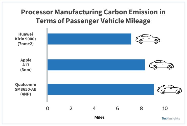
To illustrate the impact of these semiconductor carbon emissions in practical terms, the U.S. EPA states that an average passenger vehicle emits roughly 400 grams of CO2 per mile. When comparing semiconductor manufacturing carbon emissions intensity by die, the carbon from one Kirin 9000s chip would be equal to transporting you approximately seven miles, while the A17 and Qualcomm SM8650-AB would take you over eight and nine miles, respectively (Figure 2).

Figure 2. Processor Manufacturing Carbon Emissions in Terms of Passenger Vehicle Mileage. Source: TechInsights’ Semiconductor Manufacturing Carbon Model, 2024. EPA.
Now some people might question whether saving the equivalent of two miles of vehicle carbon emissions is truly significant. It’s a valid challenge. But when you factor in that TechInsights expects 1.16 billion new smartphones shipped in 2024, that two-mile savings turns into the same carbon emissions that would be released driving a passenger car more than 46,000 times around the globe.
No single phone or phone maker controls the market, but these three have a significant footprint. According to TechInsights’ forecasts, there will be nearly 43 million iPhone 15 Pro Max sold in 2024, 15 million Samsung GS24 Ultra, and approximately one million Huawei Mate 60 Pro+.
Looking more closely at the manufacturing emission profiles of the processors, although the Kirin 9000s has the lowest total emissions per die, the A17 and the Qualcomm SM8650-AB processors, both have substantially less Scope 1 emissions (Figure 3). Notably, the A17 and Qualcomm SM8650-AB chips benefit from 90% fab abatement efficiencies at TSMC, whereas SMIC's abatement efficiency is 60%.
Indirect emissions associated with the purchase of electricity for the A17 and Qualcomm SM8650-AB overwhelmingly drive their carbon footprints, accounting for ~80% of their manufacturing emissions. Another contributor to electricity emissions for these chips is Taiwan’s energy mix utilized by TSMC, which was more carbon intensive in 2023 than China’s according to Our World in Data.
Figure 3. Processor Manufacturing Emissions by Die. Source: TechInsights’ Semiconductor Manufacturing Carbon Model, 2024.
What is driving electricity consumption for the Qualcomm SM8650-AB and A17 manufacturing processes? The answer lies in three words: extreme ultraviolet (EUV) lithography. When EUV was first implemented at TSMC for its 7nm+ process, it streamlined manufacturing by replacing multiple deep ultraviolet (DUV) exposures and additional patterning steps. Despite its advantages, EUV systems consume over 10 times more electricity per system compared to DUV lithography.
Multi-patterning, this time with EUV, was again required with the transition to 5nm, reversing some process efficiencies gained from the previous generation. For the A17 processor, EUV lithography equipment electricity consumption increases 100%, with other equipment and facilities electricity usage climbing 7%, resulting in total electricity usage for the 3nm process to be 18% higher than the 4NP process on a per wafer basis (Figure 4). Examining the emissions profile by die (the yellow line in Figure 4), a familiar pattern emerges: the Qualcomm SM8650-AB, boasting the larger die, demands the highest electricity consumption on a die basis, followed by the A17 and Kirin 9000s.
There is a trade-off between the most advanced technology and emissions. While the Kirin 9000s is the lowest in terms of emissions, it also lags the A17 technology node by several generations. How Huawei’s processors will advance in the coming years is particularly interesting, with Western sanctions currently in place intended to prevent the advancement of EUV technology in China. It is possible for Huawei to make further advancements based on DUV lithography, however the drop-off in die yield is likely to be dramatic.
Figure 4. Processor Manufacturing Electricity Usage. Source: TechInsights’ Semiconductor Manufacturing Carbon Model, 2024.
It is recognized that there are hundreds of semiconductors in smartphones which have their own carbon footprint. In this preliminary analysis, it was found that process node, fab location, and abatement efficiency have a strong impact on semiconductor emissions from manufacturing. However, die size had the most significant impact on the carbon intensity on the processors evaluated. An opportunity exists for Scope 2 emissions associated with the A17 and Qualcomm SM8650-AB to be significantly lowered by utilizing lower carbon electricity.
While a phone’s processor may be more carbon intensive relative to its peers, a competitor’s handset may offer a smaller carbon footprint when the entire phone is considered. TechInsights is currently working on tools to make this data and assessment possible, and soon consumers will be able to evaluate their next smartphone purchase based not just on camera resolution and processor speed, but also on whether the phone aligns with their own sustainability goals.
About TechInsights’ Semiconductor Manufacturing Carbon Model
The TechInsights Semiconductor Manufacturing Carbon Model is the first of its kind to detail Scope 1 and Scope 2 carbon emissions at a wafer and die level. This is achieved by bringing together the equipment, processes, and manufacturing steps for Logic, DRAM, and NAND into a single tool for leading 300mm wafers produced by 184 total fabs. The tool allows users to create their own unique analyses of carbon emissions through editable fields like utilization, abatement, and electric carbon intensity.
Start My Free TrialPlatform Member? Sign In
* Please note: Certain analysis is complimentary with a TechInsights Platform trial account.
1 CO2e is the measurement unit for the impact of different GHGs on global warming in terms of the amount of CO2 calculated based on their GWP.


