Hybrid Bonding: Unpacking the Environmental Footprint of Next-Gen Memory
7 Min Read May 29, 2025
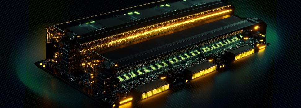
The semiconductor industry's relentless drive for greater integration and performance is ushering in a new era of complexity in semiconductor products, with hybrid bonding at its forefront. This disruptive technology, initially seen in CMOS image sensors, is now critical for high-performance computing (HPC) and advanced memory solutions like High Bandwidth Memory (HBM). While hybrid bonding undeniably enables denser, more complex integrated circuits and facilitates the shift towards chiplet architectures, its environmental implications, particularly concerning carbon emissions, warrant a closer look from sustainability professionals.

A key factor in the environmental impact is the sheer volume of silicon enabled by hybrid bonding. As die stacks within HBM grow – potentially reaching 24 die per stack by the end of the decade – the associated emissions, predominantly from the die itself, can more than triple. This increase is primarily driven by the greater amount of silicon required per product. It's crucial to understand that the hybrid bonding process itself doesn't add significant emissions; rather, it's the additional silicon density it facilitates that drives up the product’s overall carbon footprint.
The adoption of Extreme Ultraviolet (EUV) lithography for advanced DRAM chips within HBM will also contribute to Scope 2 emissions (from electricity consumption). However, this impact is generally less pronounced compared to advanced logic manufacturing, as DRAM typically avoids the extensive multi-patterning required in multiple metal layers for logic. Encouragingly, advancements in memory density, such as the transition from 2GB to 3GB dies, can lead to a reduction in emissions when measured on a per-gigabyte basis, highlighting efficiency gains.
Different hybrid bonding approaches also have varying sustainability implications. While wafer-to-wafer (W2W) bonding is more established, it cannot filter for known good die. Die-to-wafer (D2W) bonding, though more complex, allows for known good die selection, which is vital for high-yield, large-die HPC applications. From a sustainability perspective, higher yield directly translates to lower emissions per functional die, making D2W particularly productive for minimizing waste.
The demand for HBM, especially for AI applications, is projected to experience explosive growth, with market revenue potentially reaching nearly $120 billion by 2029. This insatiable demand will continue to drive up silicon intensity. For sustainability teams, the focus must extend beyond the bonding process to the broader manufacturing ecosystem. Mitigating the environmental impact of these advanced memory solutions will require a multi-faceted approach, including improved gas abatement technologies, increased reliance on renewable energy for fabrication facilities, and a concerted effort to establish a low-emissions supply chain throughout the entire semiconductor value chain.
For details and emissions data on specific HBM die stacks, read the full TechInsights report: Hybrid Bonding Increases Complexity and Carbon Intensity


