![]()
Assembly and Test Cost and Price Model
In-depth cost and price model for advanced package types including multi-die applications.
This model caters to a diverse spectrum of clientele, spanning from Integrated Device Manufacturers (IDMs) and fabless semiconductor companies to analysts, consultants, electronic systems firms, automotive enterprises, and beyond.
To understand this evolving landscape, you need a strong industry-leading business analysis tool.


Market Analysis Solutions
End Market Analysis:
The Semiconductor Manufacturing Economics Advantage
These products give any organization unique and detailed insights into the semiconductor supply chain. Customers include the world’s largest IDMs, foundries, fabless, electronics systems, automotive companies, equipment OEMs and materials suppliers, analysts, universities, and start-ups.
Supported Assembly Processes:
Leadframe, organic substrate (such as BGA, PGA, and LGA), ceramic substrate, wafer level, and InFO, including multichip and chiplet packages.
Supported Wafer Size:
75mm, 100mm, 125mm, 150mm, 200mm, and 300mm.
Supported Cost Elements:
Overall wafer sort, assembly and final test cost, assembly and tests processes, plus material usage.
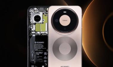
Huawei Mate 80 Pro Max Teardown Confirms Kirin 9030 Pro on SMIC N+3
TechInsights’ teardown of the Huawei Mate 80 Pro Max confirms the Kirin 9030 Pro on SMIC’s N+3 process and reveals major upgrades in display, cameras, and connectivity.
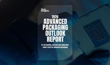
2026 Advanced Packaging Outlook Report
Discover the five expectations defining advanced packaging in 2026, including CPO adoption, HBM4 demand, panel and glass scaling, 3D thermal challenges, and chiplets for mobile.
Trump Approves H200 Exports: Impact on NVIDIA, TSMC & HBM
Trump’s approval of H200 exports to China could reshape GPU, packaging, and HBM markets. TechInsights analyzes supply constraints, pricing, and $40–50B demand.
![]()
The Authoritative Information Platform to the Semiconductor Industry.
