![]()
Strategic Cost and Price Model
Advanced and future semiconductor manufacturing processes model.
This model offers insights into advanced and future semiconductor manufacturing processes, including process specifics, equipment, material sets, detailed requirements, usage guidelines, and costs. It caters to clients such as IDMs, consortia, materials companies, and OEMs involved in market projections and costs, among others.

To understand this evolving landscape, you need a strong industry-leading business analysis tool.


Market Analysis Solutions
End Market Analysis:
The Semiconductor Manufacturing Economics Advantage
These products give any organization unique and detailed insights into the semiconductor supply chain. Customers include the world’s largest IDMs, foundries, fabless, electronics systems, automotive companies, equipment OEMs and materials suppliers, analysts, universities, and start-ups.
Model Covers:
2D and 3D NAND Flash, DRAM, Foundry and IDM Logic, and Silicon Photonics.
Supported Wafer Size:
300mm.
Supported Cost Elements:
300 wafer cost and price only.

Huawei Mate 80 Pro Max Teardown Confirms Kirin 9030 Pro on SMIC N+3
TechInsights’ teardown of the Huawei Mate 80 Pro Max confirms the Kirin 9030 Pro on SMIC’s N+3 process and reveals major upgrades in display, cameras, and connectivity.

2026 Advanced Packaging Outlook Report
Discover the five expectations defining advanced packaging in 2026, including CPO adoption, HBM4 demand, panel and glass scaling, 3D thermal challenges, and chiplets for mobile.
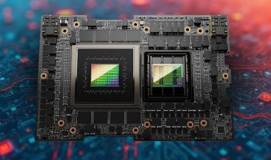
Trump Approves H200 Exports: Impact on NVIDIA, TSMC & HBM
Trump’s approval of H200 exports to China could reshape GPU, packaging, and HBM markets. TechInsights analyzes supply constraints, pricing, and $40–50B demand.
![]()
The Authoritative Information Platform to the Semiconductor Industry.
