Packaging + Carbon Module
A Cradle-to-Gate Tool for Assessing Carbon Impact
The Packaging+ Carbon Module is an industry first and enables users, in just a few seconds, to calculate the packaging carbon impact of an integrated circuit (IC) product from cradle-to-gate.
The Packaging+ Carbon Module gives IC designers, IDMs, and product manufacturers the data and tools they need to make informed decisions about product designs and component-level carbon impacts.
Data and calculations available include:
- Standardized and repeatable semiconductor carbon emissions reporting for integrated circuits, including packaging
- Single click cradle-to-gate reporting for more than 30,000 IC products analyzed and inventoried by TechInsights – across consumer, enterprise, and automotive applications
- Detailed die data, including emissions and individual die information (description, number, manufacturer, node category, function and size) for multi-chip products
- Comprehensive views of Scope 2 and Scope 3 emissions generated from chip packaging, including 3D IC integration and system-on-a-chip (SoC)
- Data on more than seventy Scope 3 materials used in packaging
- Transportation carbon calculated automatically based on weight of materials used to manufacture and package the die(s), and shipping packaging
- Over 780 assembly processes covered, with 124+ pre-configured package types that can accommodate 11 unique die
This module works in concert with TechInsights’ Manufacturing Carbon Module and Carbon Analyzer Module to leverage TechInsights' industry-leading expertise in reverse engineering and semiconductor manufacturing processes. Our proprietary databases combined with in-depth analysis and expertise provide the industry’s most comprehensive and reliable data available.

A Single Product for Cradle-to-Gate Sustainability Insights
EcoInsights is a comprehensive solution designed to help semiconductor companies drive significant environmental progress. With EcoInsights, users can quickly calculate the carbon footprint of over 30,000+ integrated circuits (ICs) with cradle-to-gate transparency. It provides detailed insights into emissions from die manufacturing, packaging, and transportation. By identifying areas for improvement, companies can make data-driven decisions to reduce their environmental impact.
This powerful suite offers three integrated modules that deliver the data and tools needed for informed sustainability choices.
The Manufacturing Carbon Module is the first of its kind to detail Scope 1, Scope 2, and Scope 3 carbon emissions by fab, location, wafer, and die. It combines equipment, processes, and manufacturing steps for Logic, DRAM, NAND, as well as select Gallium Nitride (GaN) and Silicon Carbide (SiC) processes, into a single model for over 400 fabs globally.
The Packaging+ Carbon Module lets you calculate the carbon footprint of more than 30,000 ICs with standardized calculations based on packaging type, die size, and other factors. Get detailed analysis of Scope 1 and 2 from die manufacturing and Scope 2 and 3 emissions from packaging to track the impact of your entire supply chain.
The Carbon Analyzer Module offers a product-level overview of all integrated circuits in a device and their carbon footprints, down to the packaged IC level. It simplifies benchmarking and comparing semiconductor products and manufacturers on key sustainability metrics by detailing their environmental impact at both the component and function levels.
The EcoInsights System Carbon Module bridges the gap between product design and emissions accountability. Whether you're evaluating material choices, building sustainability into your roadmap, or meeting external reporting needs, this tool puts carbon visibility in the hands of decision-makers. Evaluate the full carbon footprint of electronic assemblies using the most accessible data available.
TechInsights’ Sustainability Tools Used to Drive Down Carbon Emissions in the Supply Chain
See how best-in-class fabless vendor was able to use the Manufacturing Carbon Module to deliver a full cradle-to-gate carbon emissions analysis of nearly 100 integrated circuits (ICs) to satisfy several customers’ reporting requirements.
Packaging+ Carbon Module Opens Door to Innovative Designs
In this Module, users can run scenarios selecting from more than 30,000 IC products – across consumer, enterprise, and automotive applications - from TechInsights’ extensive databases of teardowns and reverse engineering analysis to easily provide credible data to support reporting, benchmarking, and competitive analysis. This Module currently includes 124 package types with more being added monthly. The dataset is inclusive of data from 2015 through to present. The scenarios created can be saved and used for comparison against similar or adjacent IC products.

Multichip Memory IC Product
The Packaging+ Carbon Module is part of TechInsights’ EcoInsights portfolio of Sustainability tools and insights. This Module seamlessly integrates with the Manufacturing Carbon Module and the BOM Database with Carbon Footprint, providing standardized and repeatable emissions reporting for integrated circuit products from raw materials to manufacturing to the assembly and test, and finally the transportation to deliver the parts to their destination.
Answering the Unknowns of the Carbon Impact of Chip Packaging
Whether you’re an IC designer, an integrated device manufacturer (IDM), a foundry, or a product manufacturer, the data provided by the Packaging+ Carbon Module can give you an edge in semiconductor carbon reporting. Key features include:
- Easy competitive analysis and benchmarking of carbon emissions at the IC product level
- Access to the carbon contribution of die vs. packaging vs. transportation
- Comprehensive view of Scope 2 assembly and test emissions
- Comparison of carbon emissions of the manufacturing location on an IC product's carbon footprint
- Data on more than 100 Scope 3 materials used in packaging

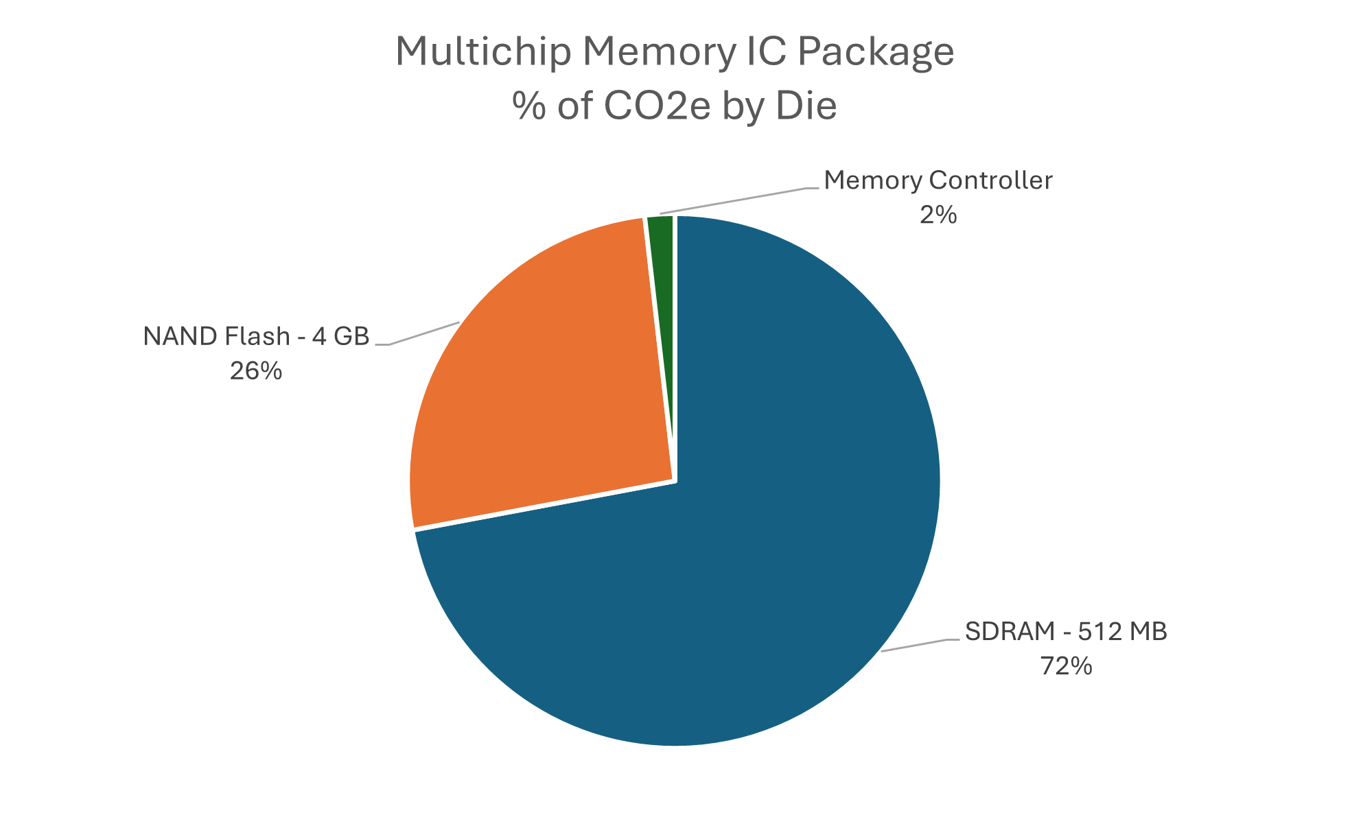
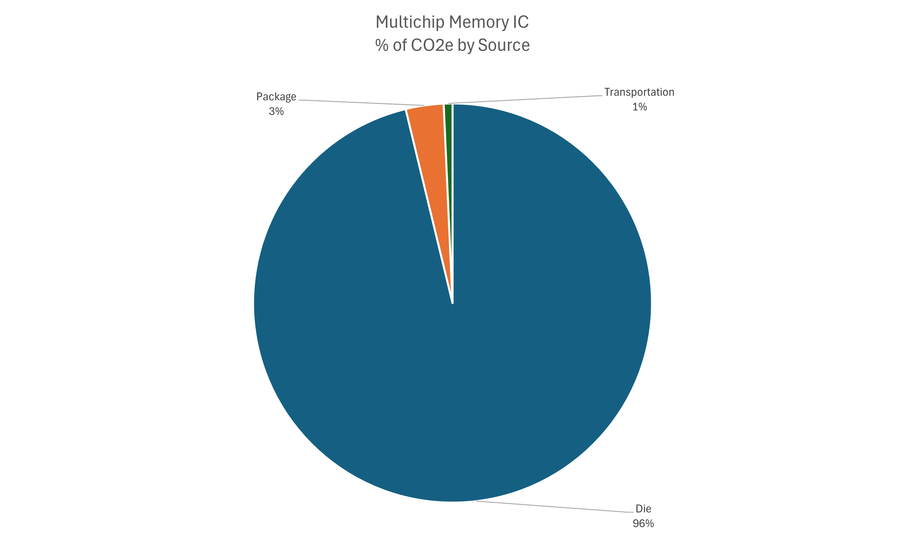
Multichip Memory IC Product
Looking at a multichip memory IC product, the majority of the CO2e comes from the manufacture of the die. Carbon by source varies significantly based on the number of die in the product, die size, number of die, die manufacturing tools and process, and package type. Source: TechInsights’ Packaging+ Carbon Module, 2024.
The Module provides IC product specific calculations of:
- Scope 1, Scope 2, and Scope 3 die emissions (manufacturing);
- Scope 2 and Scope 3 assembly emissions;
- Scope 2 test emissions;
- Scope 3 transportation emissions;
- Plus: assembly water consumption.
Get answers to key questions about semiconductor carbon impacts and how the industry is working to decrease emissions.
Supporting Your Business in Its Sustainability Reporting
Covering more than 400 fabs, the TechInsights Packaging+ Carbon Module is a vital sustainability tool providing the detailed modeling and benchmarking that supports many areas of the semiconductor value chain, including:
- Fabless Vendors can access data on transportation CO2e calculated automatically based on weight of materials used by die and in packaging for an IC product.
- Integrated Device Manufacturers can leverage "one button Cradle-to-gate" reporting for 30,000+ IC products torn down by TechInsights.
- Product Manufacturers use the data in a comprehensive view of CO2e from all IC products used in an electronic device at the touch of a button.
- Automotive Manufacturers use the comprehensive view of Scope 2 and 3 emissions from packaging, plus CO2e from die manufacturing for an IC product.
iPhone 17 Teardown Reveals Major STMicroelectronics IR Sensor Redesign
The iPhone 17 Pro Max introduces a major IR sensor redesign. See how STMicroelectronics’ new architecture reshapes biometric imaging.
Huawei Mate 80 Pro Max Teardown Confirms Kirin 9030 Pro on SMIC N+3
TechInsights’ teardown of the Huawei Mate 80 Pro Max confirms the Kirin 9030 Pro on SMIC’s N+3 process and reveals major upgrades in display, cameras, and connectivity.
2026 Advanced Packaging Outlook Report
Discover the five expectations defining advanced packaging in 2026, including CPO adoption, HBM4 demand, panel and glass scaling, 3D thermal challenges, and chiplets for mobile.


