Apple Vision Pro Utiizes SK hynix DRAM in R1 Chip
Discover how the SK hynix H5EA1A56MWA 1 Gb LLW DRAM enhances real-time processing and low-latency performance in the Apple Vision Pro AR headset with advanced memory architecture.

In the world of augmented and virtual reality (AR/VR), powerful hardware is essential for seamless real-time processing. At the heart of the Apple Vision Pro A2117 AR headset lies the Apple R1 APL1W08 sensor processing unit, which enables these immersive experiences. Central to this chipset is the SK hynix H5EA1A56MWA die, a key component that delivers the high-performance memory needed for the R1's real-time data processing, alongside the TMNB26 processor die and a second SK hynix DRAM die.
SK hynix H5EA1A56MWA in the Apple Vision Pro
The Vision Pro headset integrates high-resolution displays and sensors, relying on the Apple R1 APL1W08 chipset to deliver low-latency wide I/O (LLW) memory. The SK hynix H5EA1A56MWA die provides high memory density and power efficiency to support the demanding real-time computing needs of the headset.
The R1 APL1W08 package is manufactured by TSMC using InFO-M (Integrated Fan-Out Multi-Chip) technology, making the package compact and efficient, with 1961 solder pads. The SK hynix DRAM die fits well into this setup, offering a balance of performance and space optimization.
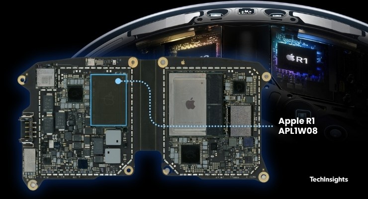
Apple R1 APL1W08 Package Location on Apple Vision Pro Mainboard
Advanced DRAM Architecture
The SK hynix H5EA1A56MWA die is built using SK hynix’s 1y nm CMOS process and features six metal interconnect layers, including tungsten, copper, and aluminum. The buried word line (WL) and bit line (BL) under capacitors technologies improve the DRAM's performance by minimizing interference and enhancing speed. Capacitors are placed between metal layers and supported by silicon nitride (SiN) storage nodes.
The die’s compact design features tightly packed lines and a small DRAM cell area, enabling high-density memory and efficient performance.
Memory Layout and Circuitry
The die consists of four identical memory circuit areas, each containing 16 memory arrays. The main peripheral circuit strip manages data and control signals and is located at the bottom of the die. This area handles most of the data path, voltage control, and bonding pads. The memory arrays and their periphery take up a significant portion of the die, with memory sub-arrays occupying a smaller but critical space.
Conclusion and Applications
The SK hynix H5EA1A56MWA 1 Gb LLW DRAM is a high-performance, power-efficient memory solution for AR/VR devices like the Apple Vision Pro. Its advanced architecture supports real-time processing, making it vital for delivering low-latency, immersive experiences.
This analysis is relevant to professionals in:
- Chip material and capital equipment supply
- Chip fabrication
- Chip design