Etch Smarter: A New Frontier in Sustainable Chip Manufacturing
5 Min Read September 12, 2025
Uncover the environmental impact of plasma etch in semiconductors and explore innovative, sustainable solutions in our report on greener etching practices.
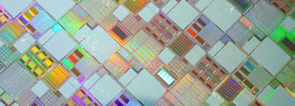
The incredible precision that allows the semiconductor industry to build chips at the atomic level comes with a hidden cost. Plasma etch, a core process in semiconductor fabrication, is one of the most energy-intensive steps in the entire workflow. Beyond consuming hundreds of kilowatts per tool, these processes rely on powerful greenhouse gases, some with a climate impact tens of thousands of times greater than carbon dioxide.
Our new report, Etch Tools Under the Microscope: Precision, Power, and Planetary Cost, reveals just how significant this challenge is, especially in complex 3D NAND production. But it also highlights the innovative solutions emerging across the industry, from low-GWP gas alternatives and energy-efficient hardware to the use of AI to optimize processes.
This isn't just a technical challenge—it's an industry-wide imperative. The path to greener etch is technically feasible, but it requires the entire ecosystem to align.
To dive deeper into the environmental footprint of processes like high aspect-ratio trenches and to explore the routes the industry can take to improve sustainability while continuing to scale, read the full report.

Understand the Impact of Plasma Etch Tools
Already registered to the TechInsights Platform? Sign in or Request Access to explore the role and impact of plasma etch tools in semiconductor sustainability.