Manufacturing Analysis Blog
The Chip Insider®
Sustainability Panel at SPIE ALP
Dan Hutcheson
March 17, 2023

Sustainability Panel at SPIE ALP: Why me? Which was my first question when they asked me to run this panel. As you know, until recently, I have considered sustainability to be a “boy scout” issue: something nice to do, but unlikely to be executed on because of the economics involved. Sustainability issues are what economists refer to as externalities: something society pays for, but the responsible parties involved do not. The only real solution to these issues is government regulation which is why the G is in ESG, which is for Environment, Safety, and Government. Government is involved in all three, except for when someone tries to squeeze sustainability into the S. The problem with sustainability is it’s a global problem and there’s no global government…
The mess is caused by something described as “The Tragedy of the Commons.” You don’t need to be an economist to understand the concept: There’s always someone who leaves their dishes in the sink, expecting someone else to clean them… It’s also why one sees net-zero by 20X0 commitments — no one wants to deal with cleaning the dishes today because it hits next quarter’s earnings. So you can see why I couldn’t get excited about doing the panel, which was in part why they asked me.
In researching it, I ran into the surprise I wrote about in the February 24th issue: OEMs and hyperverticals started to use carbon footprint in addition to price in determining which chips to buy. Then I discovered Scotten Jones of TechInsights IC Knowledge had already put carbon footprints into his cost models. That meant the OEMs and hyperverticals could take Scotten’s models and calculate the exact carbon footprint of any chip, wafer, process, or fab from the bottom up on a layer-by-layer basis. So not only were OEMs and hyperverticals using carbon footprints to make chip selections, they had the tools to do it.
With carbon footprints a part of the price, maybe a new form of ‘government’ was emerging to make executives not leave their dirty dishes in the sink. Digging deeper, I found that new form of ‘government’ was ESG and sustainability funds… it inverts Upton Sinclair’s quip that, “It is difficult to get a man to understand something when his salary depends on his not understanding it.” This is because investments by sustainability funds increase a stock’s value... Thus, it is no longer a Tragedy of the Commons failure.
The SPIE panelists did conclude that the pressure to fix sustainability was coming from the top and would be projected down into the supply chain because most emissions by OEMs and hyperverticals are Scope 3. The panel included: Aki Sekiguchi who is a Fellow in TEL’s Corporate Innovation Division, Chris Jones who is Edwards Vacuum’ Environmental Solutions Business Development Manager, Emily Gallagher who is a principal member of imec’s technical staff, John Cahill who is Senior Director of Operations and NPI Program Management at ASML Cymer; Mark Merrill who is VP of Corporate Development from Lam Research, and Ryan Russell who is corporate vice president and co-general manager of Logic Technology Development and Intel. Here’s some of each what they had to say …
Happenings, Comments, Questions & Answers: Samsung to spend 300T won ($230B) on 5 fabs
“When everything seems to be going against you …
remember that the airplane takes off against the wind” — Henry Ford
Share This Post
Sustainability Panel at SPIE Advanced Lithography and Patterning:
Why me? Which was my first question when they asked me to run this panel. As you know, until recently, I have considered sustainability to be a “boy scout” issue: something nice to do, but unlikely to be executed on because of the economics involved. Sustainability issues are what economists refer to as externalities: something society pays for, but the responsible parties involved do not. The only real solution to these issues is government regulation which is why the G is in ESG, which was for Environmental, Safety, and Government, though some change safety to social. Government is involved in all three, except for when someone tries to squeeze social and sustainability into the S. The problem with sustainability is it’s a global problem and there’s no global government. And if you question that, just look at the mess around the 2016 Paris Agreement.
The mess is caused by something ecologist Garrett Hardin described in his groundbreaking paper, “The Tragedy of the Commons,” using ideas first developed in 1833 by British economist William Forster Lloyd. You don’t need to read the paper to understand the concept: There’s always someone who leaves their dishes in the sink, expecting someone else to clean them. Office refrigerators are also a common example of The Tragedy of the Commons. It’s also why one sees net-zero by 20X0 commitments — no one wants to deal with cleaning the dishes today because it hits next quarter’s earnings. So you can see why I couldn’t get excited about doing the panel, which was in part why they asked me.
In researching it, I ran into the surprise I wrote about in the February 24th issue: OEMs and hyperverticals started to use carbon footprint in addition to price in determining which chips to buy. Then I discovered Scotten Jones of TechInsights IC Knowledge had already put carbon footprints into his cost models. That meant the OEMs and hyperverticals could take Scotten’s models and calculate the exact carbon footprint of any chip, wafer, process, or fab from the bottom up on a layer-by-layer basis. So not only were OEMs and hyperverticals using carbon footprints to make chip selections, they had the tools to do it.
With carbon footprints a part of the price, maybe a new form of ‘government’ was emerging to make executives not leave their dirty dishes in the sink. Digging deeper, I found that new form of ‘government’ was ESG and sustainability funds,1 which control something like 40% of all the funds investing in stocks. It’s a new form of government because it inverts Upton Sinclair’s quip that, “It is difficult to get a man to understand something when his salary depends on his not understanding it.” This is because investments by sustainability funds increase a stock’s value. Since stocks are a key form of compensation there are clear incentives to address sustainability. Thus, it is no longer a Tragedy of the Commons failure.
The SPIE panelists did conclude that the pressure to fix sustainability was coming from the top and would be projected down into the supply chain because most emissions by OEMs and hyperverticals are Scope 3. The panel included: Aki Sekiguchi who is a Fellow in TEL’s Corporate Innovation Division, Chris Jones who is Edwards Vacuum’ Environmental Solutions Business Development Manager, Emily Gallagher who is a principal member of imec’s technical staff, John Cahill who is Senior Director of Operations and NPI Program Management at ASML Cymer; Mark Merrill who is VP of Corporate Development from Lam Research, and Ryan Russell who is corporate vice president and co-general manager of Logic Technology Development and Intel. Here’s some of each what they had to say:
Emily Gallagher of imec led off, who sees a merging of technology details with patterning requirements becoming an industry imperative. This is especially critical as scaling pressures continue. Emily noted the many ambitious pledges to reach carbon neutrality or net-zero in the next few decades, which include: Apple net-zero by 2030, Amazon net-zero by 2040, Intel net-zero by 2040, Samsung Electronics net-zero by 2050, and Microsoft carbon negative by 2030 with removal of all carbon created by 2050. She said supply chains must align with these goals. Especially since legislation is coming: US Inflation Reduction Act appropriated funds for EPA to increase transparency and standards toward climate action commitments. Then there is EU climate law which, requires its countries to cut greenhouse gas emissions by at least 55% by 2030 with a goal of the EU being climate neutral by 2050.
Emily’s view was that sustainability has to be a ground-level change that improves the cost struggle, not hurts it. She sees more need for green energy, with on-site energy production and governmental support.
With all this pressure, she said the Paris Agreement doesn’t work. One of her big worries is that the complexity of new technologies increases with each technology node. As a result, the CO2 emissions associated will approach a doubling in the next 10 years. At the same time, the total volume of wafers produced will grow, resulting in a doubling of the volume produced in the next 10 years. If we do nothing, the emissions associated with the manufacturing of ICs will quadruple in the next decade. BUT according to the Paris agreement, all industry sectors should work on cutting their emissions in half every decade. In other words, in the “do-nothing” scenario, our industry will be off target by a factor 8... Even with the rollout of clean energy at the current rate we will be 2.5 times off target.
Emily’s recommendation for this community is that we must assess the environmental impact at all stages: “PPACE” Power Performance Area Cost and Environmental. Measure what you need to change. Work with the entire semiconductor supply chain, together, providing our partners with better insights – supported by data. Identify high-impact problems and guide green technology pathfinding. Work with organizations like SEMI, SRDC for common reporting and sharing of solutions. On that note, imec recently became a founding member of the semiconductor climate consortia or SCC. Everyone is needed to develop and enable new solutions which will help us reach net-zero emissions before 2050.
The big issue she sees as having an impact at the ground level is developing consistent measuring and reporting standards for the environmental footprint. Also developing a proactive approach where environmental considerations are placed in the early stages of technology definition. Imec has initiated its SSTS (Sustainable Semiconductor Technology and Systems) to quantify the environmental impact of IC manufacturing of future logic & memory devices. The goal is to identify areas of high impact and work towards solutions in these areas. They are working on a virtual fab — imec.netzero — that can help to create a common language for data reporting and sharing and enable data-driven policy, based on independent and transparent data. She said a public version of imec’s virtual fab would be available later this year.
Aki Sekiguchi of TEL pointed out that sustainable technology development has been a company-wide activity for many years. This should come as no surprise since they are a Japanese company. I’ve dealt with TEL for decades and they’ve always had a deep sense of social responsibility. TEL’s efforts span scopes 1, 2, and 3. Needless to say, they have their own activities in addition to joint activities with suppliers and customers.
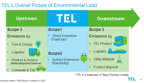
Personally, Aki sees the challenge as “daunting,” pointing out that TEL’s Scope 1 and 2 emissions are a mere 0.3%, drawing on a presentation from Mitano-san at SEMI’s ITPC conference. Scope 1 and 2 are the emissions you have a direct influence over. Upstream Scope 3 emissions are just 2%. The problem is downstream 3 emissions, which represent 98% of all TEL’s emissions. I suspect it’s little different for the rest of the equipment industry.
Aki believes TEL is in a unique position to influence the solution. As he puts it, Tokyo Electron is one of the few companies engaged in all aspects of patterning which places it in a unique position to optimize PPACE(nvironment) holistically. TEL needs to do more than just optimize track. Different tools have different footprints: Etch is electricity intensive. Wet Stations, Water. Track is Chemical. And Furnaces are Facility and Electricity centric. Aki’s formula for success is:
Environmental performance = equipment performance
Which is driven by Mitano-san’s E-COMPASS model: Environmental Co-Creation by Material, Process and Subcomponent Solutions
The expose-track tools are part of this company-wide holistic approach to sustainability. Patterning is a holistic approach. New chemistries to reduce dose, such as metal-oxide resists.
Mark Merrill of Lam Research started out with the company’s public roadmap to achieve net-zero emissions with an eye to social responsibility with science-based targets. Regarding their goal to reduce Scope 1 and 2 emissions, they expect to achieve a 25% reduction from their 2019 baseline by 2025 and a 46% reduction by 2030, with a 100% reduction by 2040. By 2030 they will use 100% renewable electricity. In terms of Scope 3 value-chain emissions, they are expecting 46.5% from top suppliers by 2025 and 95% of top suppliers by spend by 2030. By 2050 they plan to achieve net zero emissions in all scopes. Impressively, Lam’s near-term greenhouse emissions reduction targets have been approved by the Science Based targets initiative (SBTi), making Lam the first U.S.-based semi equipment manufacturer to be approved. Additionally, Lam Capital — its Venture Capital arm — is sponsoring and funding ESG based technologies for the Semiconductor market. They are funding next gen tech that saves on energy space.
Lam is also approaching sustainability as a product designer and producer: As part of thier development process, they now require each program to outline ESG goals and Key Performance Indicators. Proof of results is the new Sense.i platform which reduces the total amount of raw aluminum by 15,000 lbs. for every Sense.i tool shipped. They did this by going from a traditional cluster-tool clover-leaf layout to a stacked platform, which also uses less cleanroom space. Specifically for lithography, Lam’s dry resist development approach offers sustainability benefits by consuming less energy and five to ten times fewer raw materials (including fewer chemicals).
John Cahill of ASML Cymer gave an overview of their reclaim process, as it off-sets a significant percentage of their potential spend, which enables guaranteed YoY savings for customers via On Pulse service pricing. Cymer re-uses nearly 900,000 pounds in parts annually to reduce the environmental impact of its suppliers. That is equivalent to what’s in 11 New York City Subway Cars. In order to ensure quality, all reclaim/re-use parts must meet “As new specifications” and pass all testing requirements. Cymer tracks all module life-times and has shown that reclaim parts show no reduction in life-time.
They are also proactive. The ultimate reclaim/re-use goal should be a never-ending pursuit to design and introduce modules that last longer than the prior generations. Johns points out that longer replacement intervals mean reduced service events and their associated environmental impact. Longer life modules increase system availability and translate to additional wafer passes-per-year while reducing environmental impact. This way Cymer is able to execute sustainability that reduces Cost of Operation. He said the results so far indicate around a ~55% reduction in ArFi facility CoO and ~40% reduction in KrF facility CoO.
Chris Jones of Edwards believes it’s no longer an issue of the industry recognizing the importance of emissions to control climate change. We do! Chris also emphasized the top-down sustainability economic model, saying Scope 3 upstream emissions will drive the desire to buy from suppliers whom themselves have a low carbon footprint, which is what Edwards is doing.
Challenge for an industry that wants to grow implies they need to halve emissions. Chris said manufacturing emissions are mainly about energy and process gases. Fabs are big energy users – EUV Lithography is no exception - Low carbon energy is becoming increasingly available, but it’s patchy based on where major user fabs are. Chris said, sometimes, reality is better than perception. EUV may have a bad reputation. But it has reduced etch steps, netting a much smaller carbon footprint when looked at holistically.
Also, abatement companies are all working to improve their performance to reduce emissions further. Chris said we can't continue vacuum and abatement with the current paradigm. First is to use the right energy to destroy those gases, but only when needed. Chris also sees an increasing emphasis on the use of green materials – but at a cost, and there may be a market shortage further driving cost increases. He cautions us to remember that it’s about legal compliance first, then cost, and then emissions.
He’s also a big believer in next-generation technology as a solution. Lithography needs lots of energy and hydrogen, which itself uses a lot of energy. That’s why they have developed a hydrogen recycling technology, which has been tested out and is working at imec.
Ryan Russell of Intel brought the chipmaker perspective. But more importantly, he brought the personal view of someone who understands the problem through the lens of the families it impacts near Intel’s fabs and around the globe.
Intel has long believed in sustainable business practices. Back in 1994 it took the lead in reducing PFCs and in 1996 it started a renewable energy push. I remember that Intel was a big partner to the EPA when the latter was dealing with the Fairchild underground storage leak in South San Jose, proving the EPA with metrology tools they didn’t have. Ryan emphasized that these efforts are a must-do for Intel’s success as well as the communities where it operates. Ryan said this helps mitigate risks, reduces costs, and builds brand value while benefiting us all.
Still, Ryan said new approaches are needed in order to ensure growth doesn’t offset progress. Breakthrough solutions will be needed to continue reducing impact.
As Intel expands its manufacturing footprint Ryan is excited about opportunities around litho and other fab tooling to make a difference. Historically Intel was in the same cleanroom footprint. Given their expansion, its historic speed won’t be fast enough. As Intel scales faster, it needs to change the slope. Ryan is a big believer in proactive approaches, calling on suppliers to work together to build better tools up front. They are committed to evolving the collaboration with suppliers to collectively drive improvement and kicked off some new approaches in that collaboration starting at the end of 2022. Ryan emphasized that its partnering model has changed. There is a change of culture in process development. They now tell partners what the problem statement is upfront, rather than leaving them to guess.
Sustainability is not just a “do good” activity — chemical and water use, energy consumption, and waste disposal, all have an impact on the total cost of operations and affect the bottom line. Ryan’s thinking about sustainability is something like robbing Peter to pay Paul in a good way. Using less costs less. For example, they changed the way they ship wafers. They used to use the FOSBIES that wafers came in. They redesigned the packaging so that it’s denser and fewer wafers are damaged. The savings paid for the cost of the tool to do it in a quarter. Plus it saved 230Kg of CO2 emissions. Ryan emphasized, “Design a better tool and sell it to me. I’ll buy it.”
Innovating to develop greener chemistry solutions is imperative too. Ryan pointed to PFAS and GHGs, for example, which are coming under increased scrutiny while also being critical ingredients for semiconductor manufacturing. The industry needs to drive advances in metrology sensitivity to drive subsequent progress in materials engineering. It also needs to look at clean water versus wastewater. He issued a call to arms for the metrology industry to address these issues.
1 To give you an idea of the threat this new form of government poses, consider that the U.S. House of Representatives is planning to have hearings on what conservatives see as the “politization of investments,” according to a WSJ article on 28 Feb 2023, page A5. “Their goal: Transform the acronym for environmental, social, and corporate-governance in a rallying cry against “woke capitalism.”” The article said that 16 states are considering anti-ESG legislation.
Happenings, Comments, Questions & Answers:
Samsung to spend 300T won ($230B) on 5 fabs over 20 years (Nikkei Asia 15 Mar 23): Don’t focus on the money, because this is a big nothing burger. Nothing burgers look juicy on a monitor, but there’s nothing edible there. First, there’s no accountability to a number 20 year’s out. When 2043 rolls around, few will remember this commitment. But do the math: It’s 230B over 20 years. That’s $11.5B per year on average, but wait… Assuming a 9% CAGR spread over 20 years, the spend starts with $4.5B this year, or 14% of this year’s spending. Between now and 2030, it totals $49.6B, which is a little over 2 GFE’s (Giga-Fab Equivalents). As for 5 fabs, it’s not enough. To get to $1B by 2030, the industry will need more than 100 new GFEs (Giga-Fab Equivalent). Samsung’s spend to 2030 would only amount to 2% of the spend needed for the industry between now and 2030, causing them to lose market share. So the big number is for show, not for dough. What was really foggy here is the degree to which the South Korean Government is involved. MOTIE announced plans to spend 340T won by 2026 on semiconductors, setting up a chip cluster in Yongin. — Dan
Make informed business decisions faster and with greater confidence
Gain sample access to the world’s most trusted source of actionable, in-depth intelligence related to semiconductor innovation and surrounding markets.