Chip Observer
Tracking the market for semiconductors, from the fab floor to the customer’s door.
Latest Blogs and Commentary

Google Pixel 6 Pro Periscope Camera is a modified design of the Xiaomi Mi 10 Ultra module
In late 2021, the Google Pixel 6 Pro was launched and has been widely regarded as the best smartphone Google has made to date.
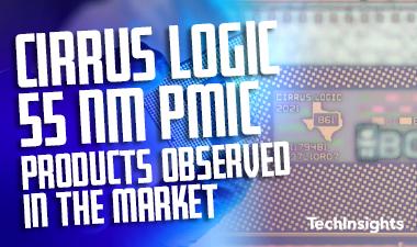
Cirrus Logic 55 nm PMIC Products Observed in the Market
In a blog written by Stephen Russell, TechInsight's Senior Process Analyst, he explains why a logic node of 55 nm is important for a PMIC and his findings of recent teardown projects.

Apple Joins 3D-Fabric Portfolio with M1 Ultra?
On March 8, Apple held their “Peek Performance” event, introducing the all-new Mac Studio and Studio Display, a new iPad Air, the new iPhone SE, and two new shades of green for the iPhone 13 and iPhone 13 Pro.
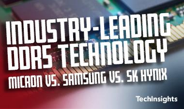
Industry-leading DDR5 Technology
We have just entered into the era of DDR5 memory. All the major DRAM players such as Micron, Samsung, and SK Hynix have started to release their first DDR5 memory products (modules) since last year.

Ray-Ban Stories smart glasses cameras
The new Ray-Ban Wayfarer Stories glasses are a product developed by Facebook in a partnership with EssilorLuxottica, and TechInsights decided to take a look at the cameras these smart glasses use.
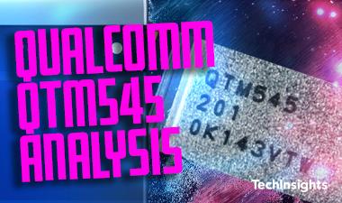
Qualcomm QTM545 Analysis
The Samsung Galaxy S22 Ultra has the latest and greatest Qualcomm mmWave, but not in Europe...

Workforce Development Solutions with SEMI
Ajit Manocha of SEMI has a conversation with Dan Hutcheson about the workforce development SEMI is accomplishing.

Innovation in Memory with Micron Technology
Scott DeBoer of Micron Technology has a conversation with Dan Hutcheson about what it takes to innovate in Memory today.

Samsung Galaxy S22 Ultra teardown
Our colleagues did a quick teardown of the Samsung Exynos 2200-powered Galaxy S22 Ultra, so we can share some of our early teardown results now.

Microsoft and Sony Acquisitions - a Strategy Game
Microsoft and Sony Acquisitions - a Strategy Game Contributing author: Peter Johnston Access the world's largest database of consumer electronics and semiconductor reverse engineering Login to the Platform Microsoft and Sony have independently

Apple AirTag Teardown
Our interest in tag trackers is how much technology has evolved. We live in a world where a device the size of a US quarter-cent piece can have multiple antennas, radio ICs, a battery and continue to operate as a two-way radio, pinpointing objects within feet of accuracy for almost a full year.
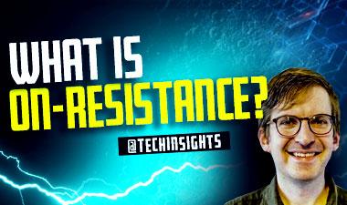
TechInsights Answers: Power Semiconductors - What is On-Resistance?
A common question our Power Semiconductor experts encounter is: What is on-resistance? Stated simply, on-resistance is the total resistance between the drain and source terminals of a FET.
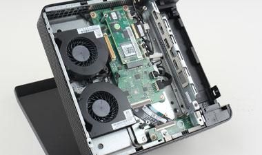
Lenovo ThinkSmart Hub Teardown
This analysis allowed us to compare or discover new manufacturers, sub-assemblies, and ICs we have found in the consumer device market with components and brands found in the business-focused ThinkSmart Hub.

Recognizing the Best Chips and Technology of the Past Year
To recognize the top semiconductor offerings of the year, The Linley Group (powered by TechInsights) presents its 2021 Analysts’ Choice Awards.
Preview of Qualcomm’s 7th generation 4G/5G Envelope Tracker QET7100
Qualcomm announced the QET7100 – the successor to the QET6100, which they dubbed the "world’s first announced 5G 100MHz envelope tracking solution."

eBook: Chevy Bolt Recall - A Battery of Problems
Discover the essential guide to the Chevrolet Bolt recall, uncovering detailed insights, impacts on owners, and the latest developments in automotive safety and electric vehicle technology.
Huawei Mate 60 Pro Mobile RF Architecture Proves They Can Compete with Top-Tier Smartphone OEMs
*Subscribers get exclusive access to additional details and annotated images.
![]()
The Authoritative Information Platform to the Semiconductor Industry.
