Posted: October 18, 2012
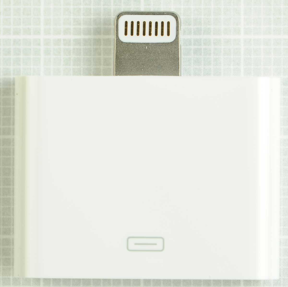
Apple Lightning to 30 Pin Adapter
Reverse engineering is not forward engineering done backwards and so you never know what you will learn or when you will learn it. Enter the Apple Lightning Adapter plug. Deserving of some analysis since we are undertaking a full systems report on this particular slice of Apple technology. To quote one of our engineers, "there is a ridiculous amount of silicon here", so when you plunk down your $30 you can feel satisfied that you are getting value-for-money.
Even without the couple hundred engineering hours involved in a systems analysis, we can at least make a few observations from the teardown.
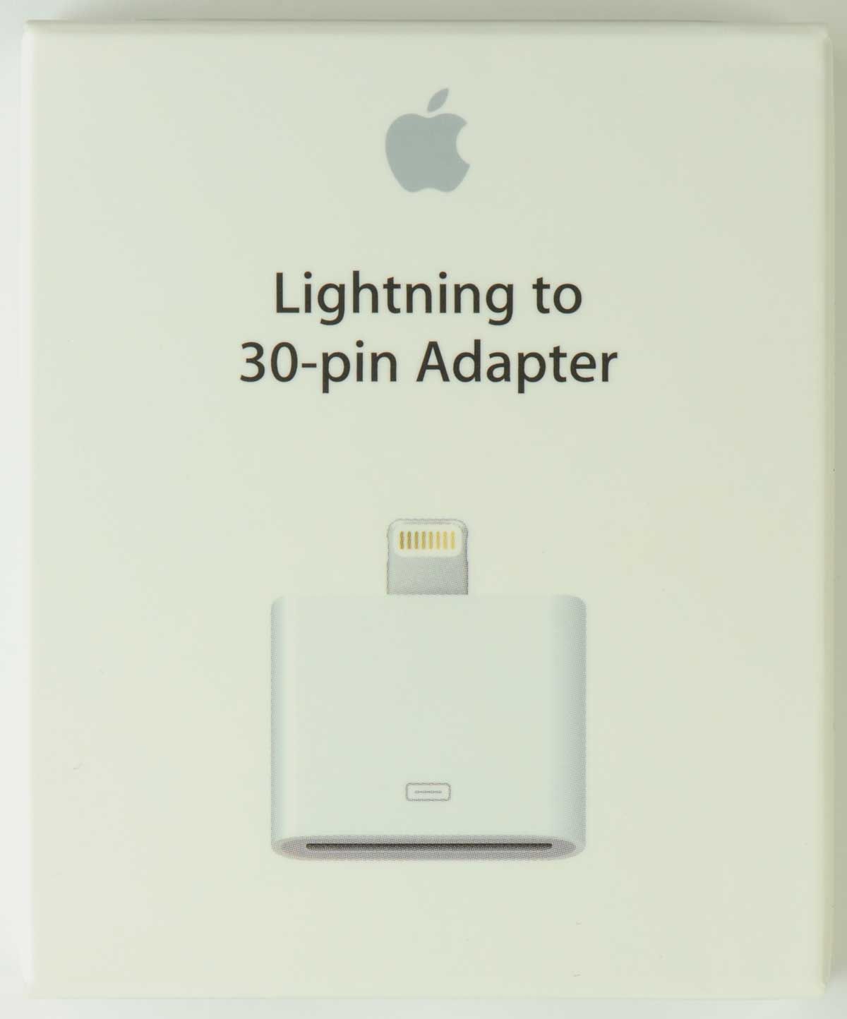
Firstly, the box features a very close approximation of what is inside it. Kudos to Apple for applying a cool brand where once it was a descriptive (boring) 30-pin adapter. At least it isn't an acronym for 8 syllables of techno-speak (USB anyone?).
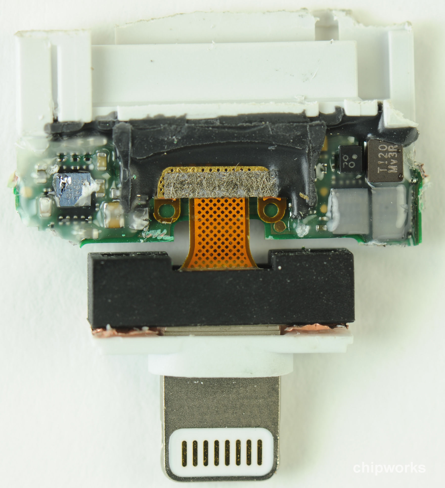
Getting inside a lot of goop
Getting inside a lot of goop
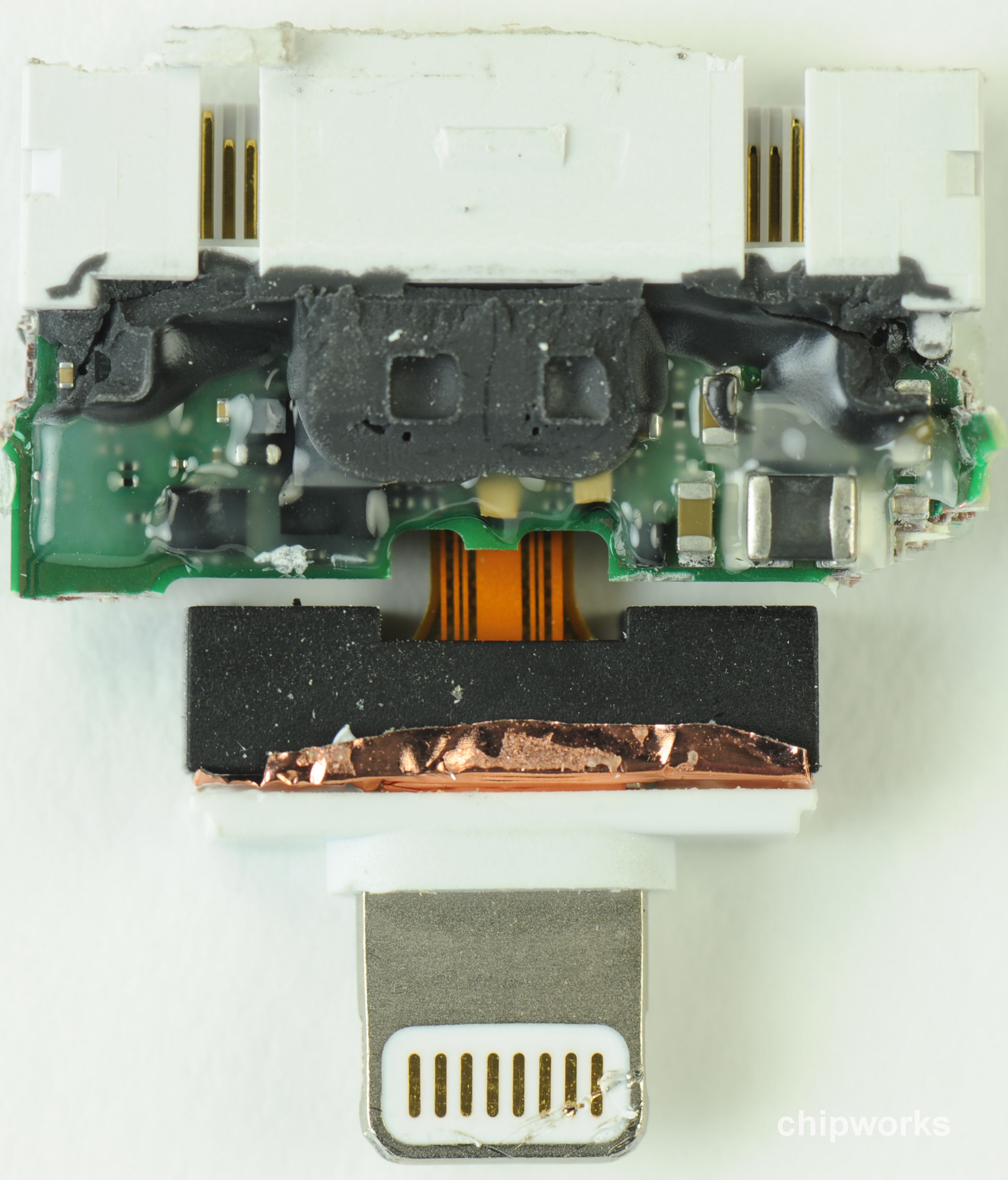
Getting the small package apart while still getting the good quality pictures needed is not easy. Once the cover is removed, we can't really see anything. A few die with markings that don't show any evidence of their manufacture. There are quite a few die for such a tiny adapter. Removing the rest of the components are where we can tell the story. The "less useful" images are at right for those interested in the blow-by-blow.
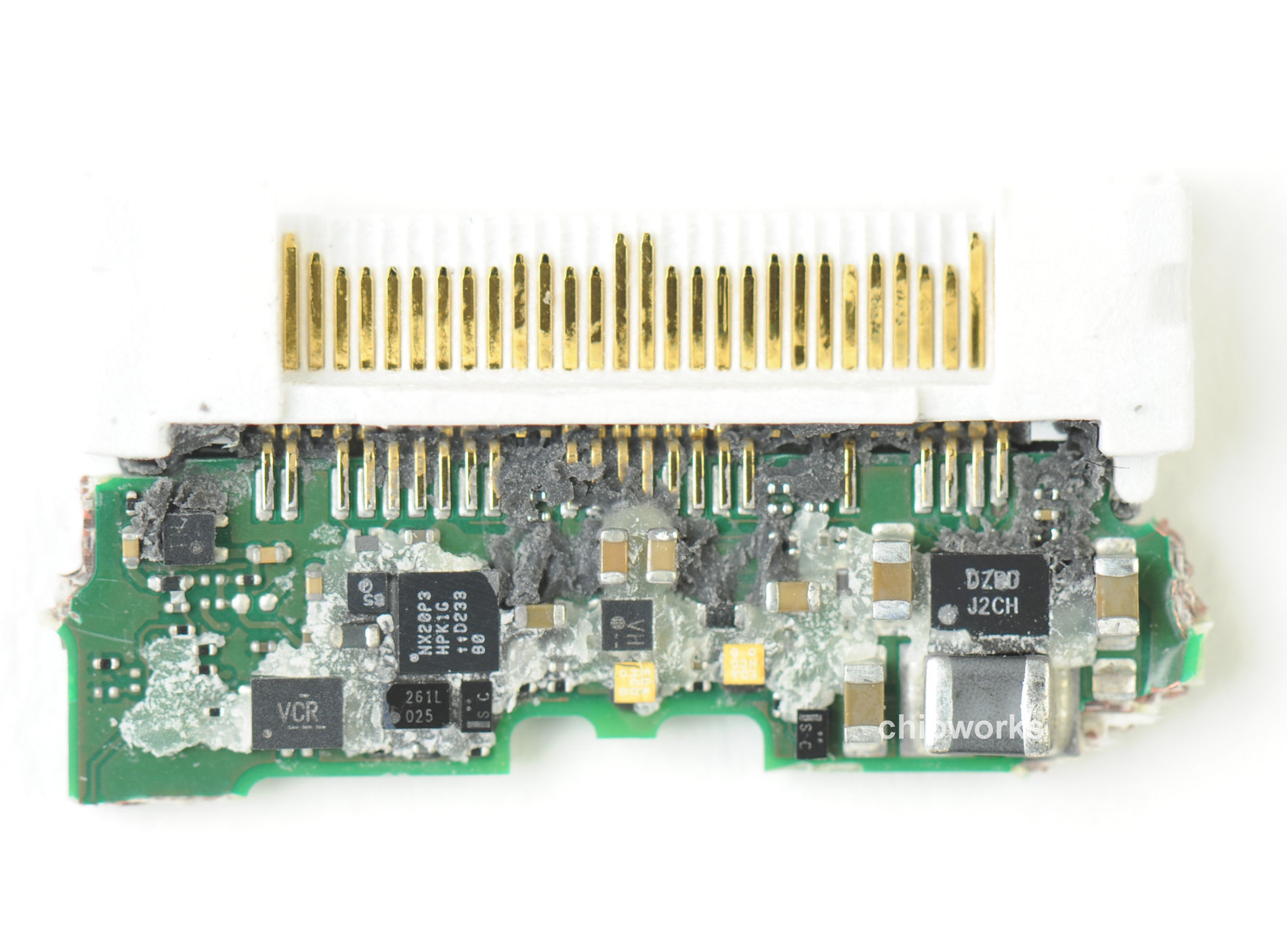
Lightning Board Side 1
Lightning Board Side 1
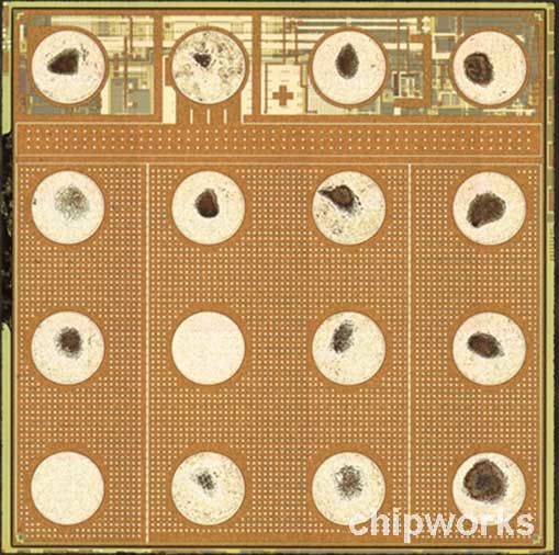
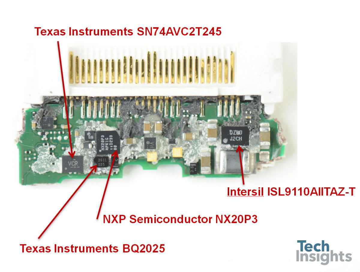
Once we have the board we can start cataloging the chips. On the one side of the board we have the same NXP20P3 that is also present in the lightning cable. It continues to present as an analog chip with very large transistors or diodes (confirmed with the polysilicon layer image). We think this is most likely an multi-channel interface filter. Again, this is looking at a die photo and not a complete RE project, but at this point we are fairly comfortable saying that.
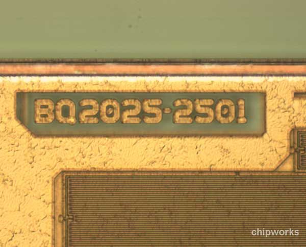
We were initially surprised by the lack of a package similar to the Texas Instruments BQ2025 that was found in the cable, but after the depot treatment it was right there in the package marked 261L025, right below the NXP chip.
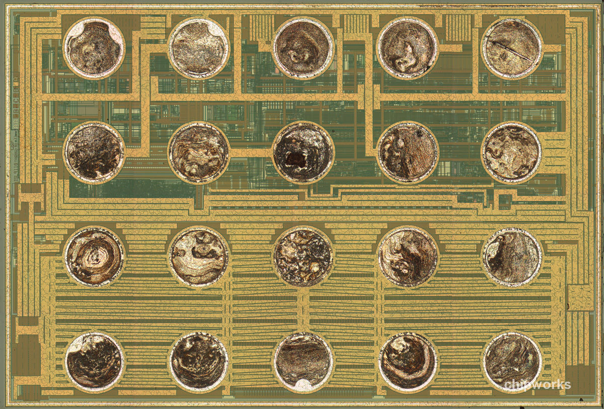
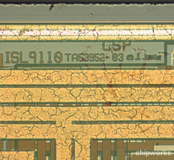
Over on the right side of the board we have the package marked DZB0J2CH with an Intersil ISL9110die inside. According to their website this is a 1.2 A High Efficiency Buck-Boost Regulator.
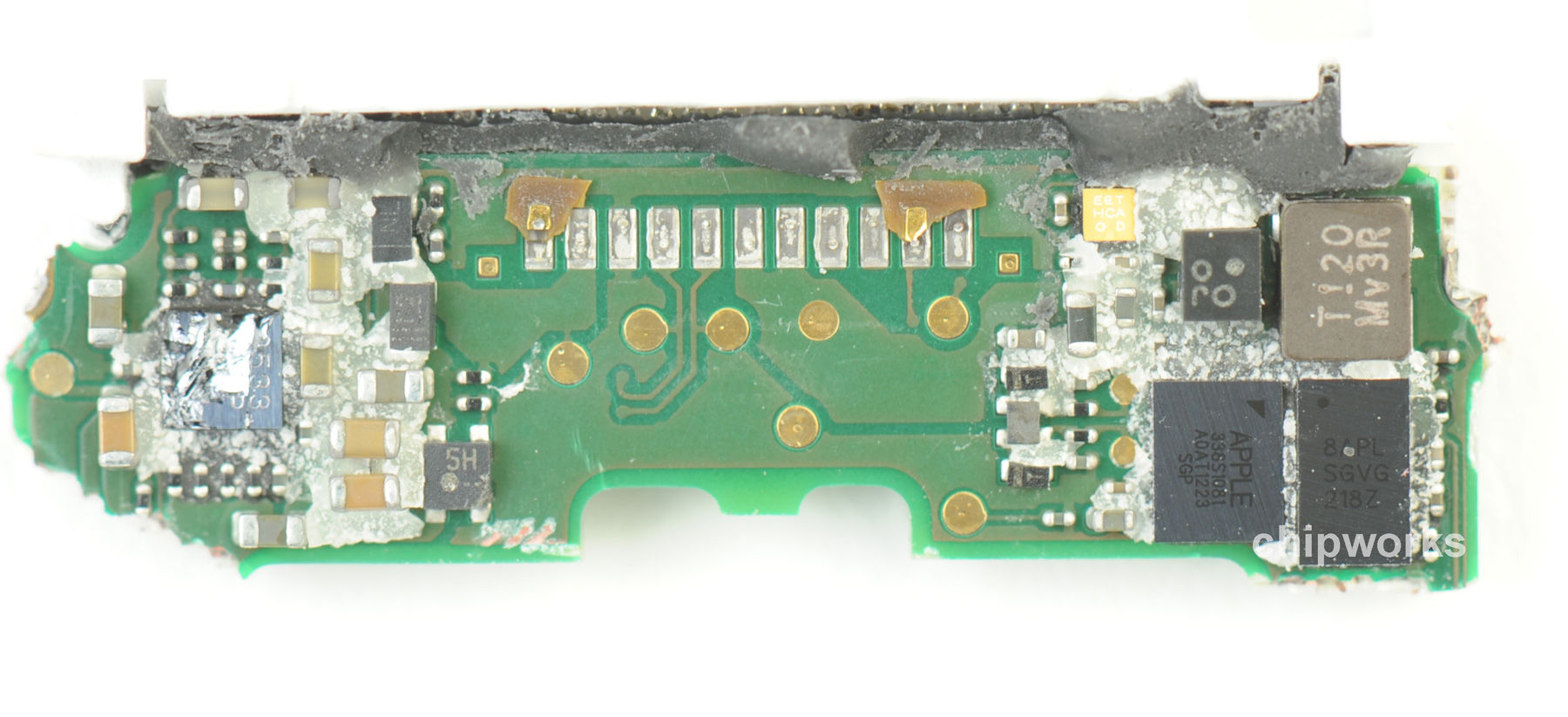
Lightning Board Side 2
Lightning Board Side 2
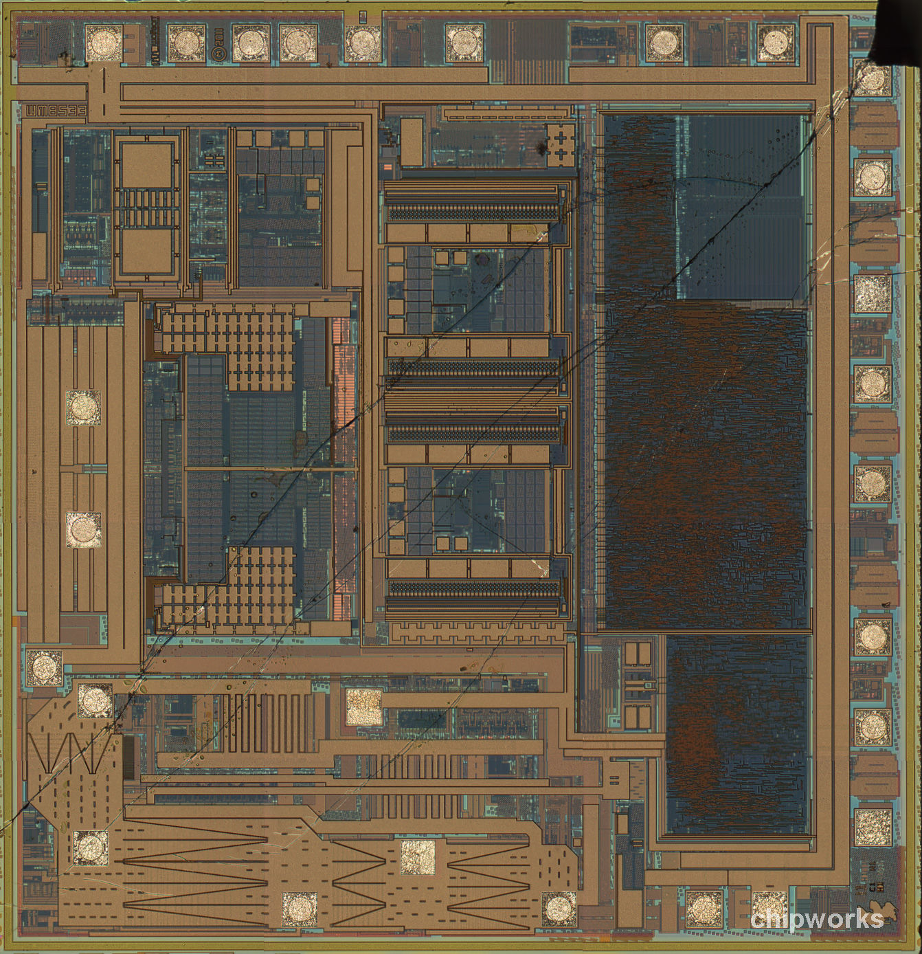
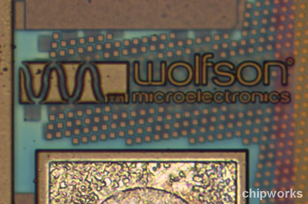
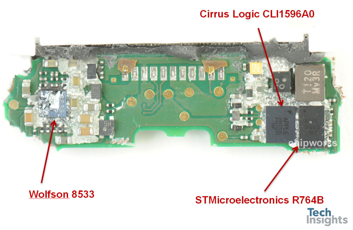
Here we have the bulk of the media devices. The Wolfson WM8533 DAC, that we think is taking the digital audio and converting it into the analog signal that the 30 pin delivers.
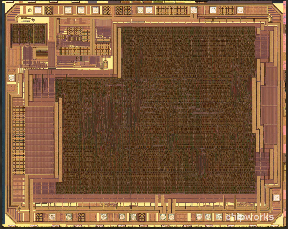
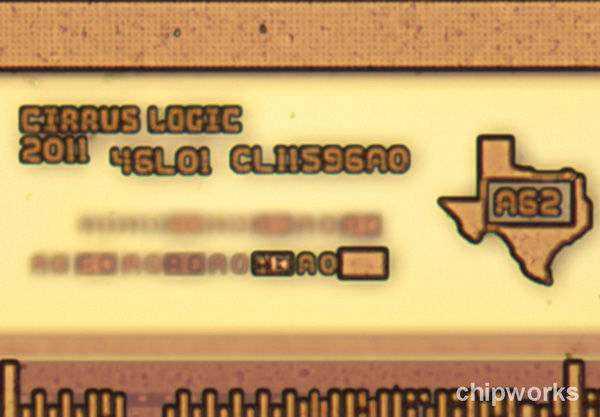
We also have the Apple 338S1081 which is a Cirrus Logic audio chip with die markings CLI1596A0 and date code 2011. For those who might be wondering as to its functionality, it didn't directly compare to the die we cataloged in the prior generations of iPhones (in the models we tore down).
No surprise is that there are no similar chips here for converting video since there is no support for video out into the older 30-pin devices. This may impact some niche peripherals out there, but you can't fight progress.
Other devices depotted
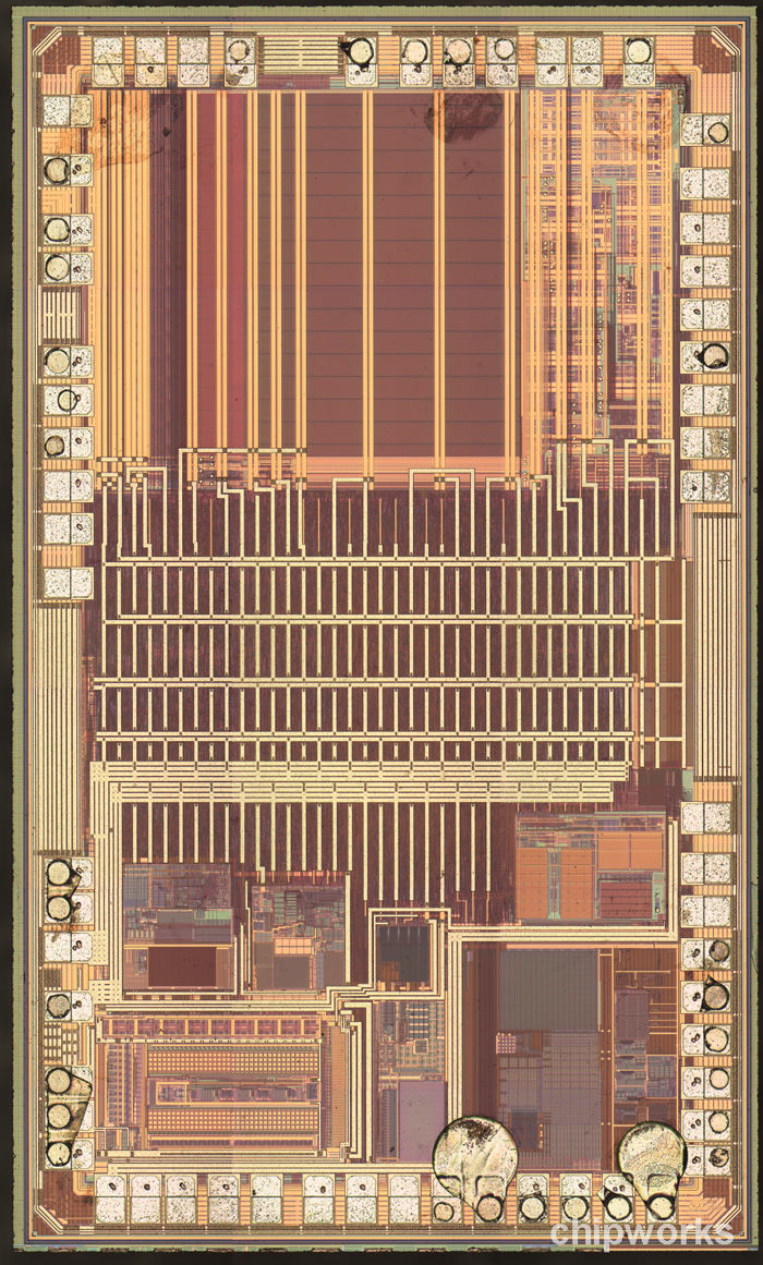
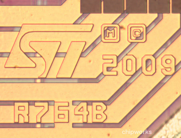
- The 8APLSGVG218Z which is an STMicroelectronics design win with die markings R764B
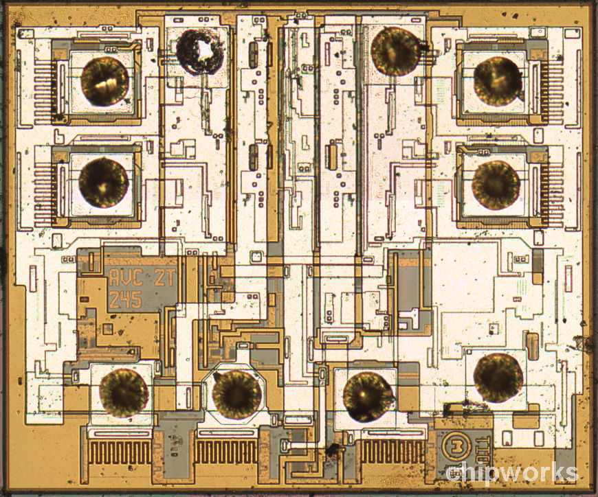
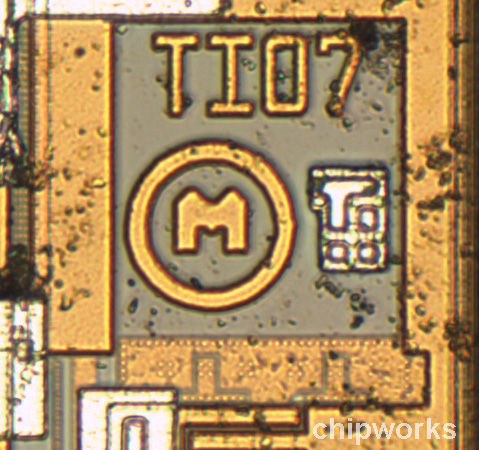
- The VCR package had a die with markings that decoded to the Texas Instruments SN74AVC2T245 dual bit non-inverting BUS transceiver
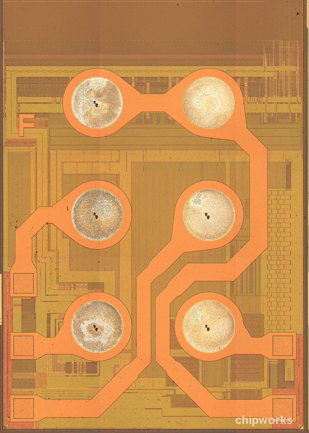
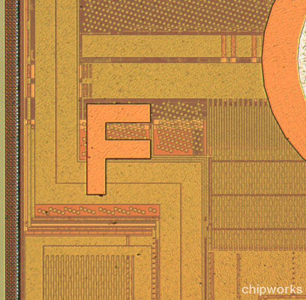
- An unknown die with the marking "F" (last one at right)
Full board shots
Other devices
Other devices


