Posted: April 11, 2018
Contributing Author: Jeongdong Choe, Senior Technical Fellow
We at TechInsights are happy to report that we have found and analyzed Anti-fuse array blocks on a Samsung 18 nm DDR4 DRAM die.
Anti-fuse is one of the embedded NVM technologies, which include:
- embedded Flash
- ROM
- eFuse (electrical fuse)
- FG/CTF Flash
- Anti-fuse
eFuse is a one-time programmable (OTP) memory that is programmed by forcing a high current density through a conductor link to make its resistance significantly higher. Anti-fuse is another OTP type NVM, but its circuit is quite different from that of eFuse. The anti-fuse circuit has a high resistance state at the beginning and is programmed by applying electrical stress in a low resistance state.
Anti-fuse NVM technology has been implemented for many decades using additional processing steps by Kilopass. Kilopass was the first to develop it in a standard CMOS process with 1T or 2T bit-cell structure.
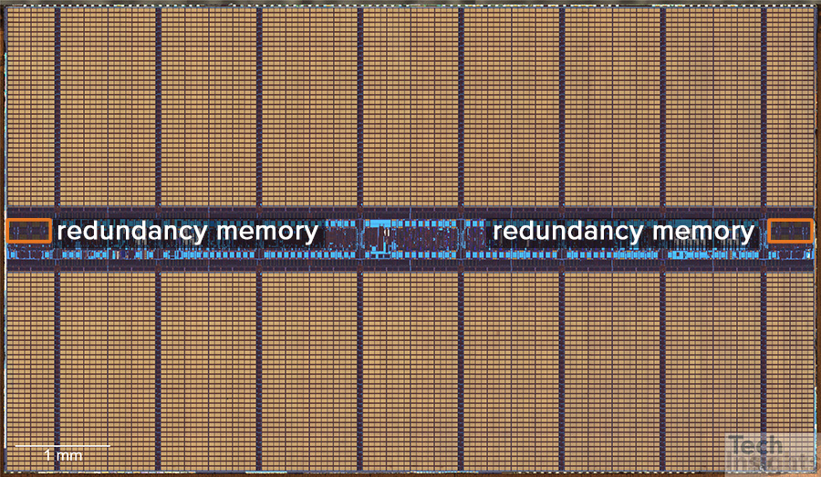
We delayered Samsung’s 8 Gb 18 nm DDR4 DRAM die to the gate level and found the anti-fuse OTP array blocks in the peripheral area. The anti-fuse blocks are located on both sides of the die as shown in Figure 1. Each anti-fuse block consists of six sub-blocks.
For anti-fuse memory technology, one or many transistors can be used for a bit cell. Samsung’s DDR4 DRAM anti-fuse bit cell structure is comprised of two transistors: a select transistor and a programmable transistor. When the programmable transistor’s gate oxide is intact, the read transistor returns a binary zero; breaking the gate creates a conductive path, returning a binary one. The wordline pitch is 0.20 µm and the bit cell area measures 0.12 µm2. TechInsights’ structural / materials / design analysis report on the Samsung K4A8G085WC-BCRC 1x nm 8 Gb DDR4 SDRAM contains more details.
Download product information on Samsung 18nm DDR and LPDDR4X
Our product information includes: Samsung K3UH5H50MM-NGCJ (LPDDR4X Mobile SDRAM) and K4A8G085WC-BCRC (DDR4).


