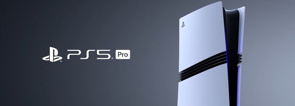
Sony PlayStation 5 Pro Teardown
Teardown Reveals Custom AMD RDNA 3.0 Processor and Boosted Memory Design
5 Min Read May 26, 2025
TechInsights’ teardown of the Sony PlayStation 5 Pro (CFI-7021) shows a strategic redesign with next-gen graphics, increased memory capacity, and modest cost increases over the PS5.
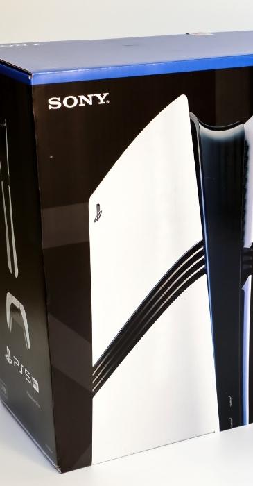
Sony has officially leveled up with the release of the PlayStation 5 Pro (CFI-7021), and TechInsights has performed a full teardown to uncover what’s powering the next-gen experience. The upgraded console, purchased in Europe, reveals a new custom processor built on AMD’s RDNA 3.0 GPU architecture, improved memory subsystems, and expanded storage — all contributing to a rebalanced bill of materials (BOM) that is just 2% higher than the standard PS5.
Custom Processor: AMD RDNA 3.0 Architecture Makes Its Console Debut
At the heart of the PS5 Pro is the Sony CXD90072GG processor, a custom chip built on AMD’s Zen 2 CPU and next-gen RDNA 3.0 GPU. This processor represents a significant architectural leap from the RDNA 2.0-based CXD90060GG found in the original PS5. Despite its enhanced capabilities, the new processor accounts for only 18.52% of the console’s estimated BOM — a notable reduction from the 30.91% cost share of its predecessor.
This lower cost impact suggests advancements in silicon efficiency or manufacturing economics, allowing Sony to pack more performance into the Pro version without a dramatic increase in production costs.
Memory and Storage: A Major Cost Driver
Memory is now the largest cost contributor to the PlayStation 5 Pro’s hardware BOM, making up an estimated 35% of total build costs. The console includes:
- 16 GB Samsung GDDR6 for GPU memory
- 2 GB Micron DDR5 and Samsung DDR4 supporting the CXD90070GG NVMe host controller
- 2 TB of Samsung 3D TLC V-NAND storage
This storage upgrade alone significantly enhances the console’s value proposition, particularly for gamers who demand fast load times and extensive game libraries.
Enhanced Connectivity: Wi-Fi 7 and Bluetooth 5.1
Connectivity also gets an upgrade, with the integration of the MediaTek MT3605AEN SoC supporting Wi-Fi 7 and Bluetooth 5.1. The cost impact of this connectivity module is higher compared to the original PS5, reflecting the adoption of newer wireless standards.
Supporting Custom Chips and Component Costs
In addition to the main processor, Sony packed the PS5 Pro with other custom silicon:
- Sony CXD90069GG Southbridge, managing HDMI and Ethernet
- Sony CXD90071GG, used in the controller
The enclosure continues to use ABS materials, and while these shell components are cheaper than those of the original PS5, the total non-electronic costs are higher in the PS5 Pro.
The Sony PlayStation 5 Pro’s engineering points to a focused effort on performance, connectivity, and memory capacity. With a modest 2% increase in estimated BOM over the original PS5, Sony has introduced meaningful upgrades while maintaining cost efficiency. The custom AMD RDNA 3.0 processor and significantly expanded memory footprint are the most impactful contributors to this next-gen console’s cost structure.
Want to see the full breakdown of components, costs, and competitive insights?
Subscribe to TechInsights and unlock in-depth teardown reports and expert insights on the world’s leading smartphones, smartwatches, and smart rings — including the full analysis of the PlayStation 5 Pro and its advanced custom processor design.