Contributed Author: Sinjin Dixon-Warren
The market for Silicon Carbide (SiC) power transistors is expected to grow considerably over the coming years. SiC power transistors have several advantages over traditional silicon-based devices, including improved performance in high-temperature, high-frequency and high-voltage applications. This makes SiC power transistors ideally suited for automotive, energy and industrial applications. As manufacturers work to meet the increased demand for SiC power transistors there is a need for innovation in manufacturing processes to reduce cost and improve performance. State of the art techniques can be used to analyze these innovations and reconstruct the sequence of steps used during the fabrication process. The resulting process flows can provide valuable insight into the equipment and materials needed in the manufacturing of SiC power transistors.
TechInsights has recently completed a full analysis of the process flow used to fabricate the Rohm SCT3022ALGC11 N-channel, SiC, trench, power MOSFET. The SCT3022ALGC11 is a 650 V, 93 A device, with an RDSON of 22 m. It is a leading etch SiC trench gate power FET, and is designed for use in solar inverters, DC/DC converters, switch mode power supplies, induction heating and motor drives.
Our analysts used their knowledge of lithography to select a region of the device for analysis that would provide the greatest insight into the manufacturing process flow, specifically a single cell of the transistor array. The region was then analyzed using a combination of techniques including scanning electron microscopy (SEM) imaging, energy dispersive x-ray spectroscopy (EDS) and scanning capacitive microscopy (SCM) imaging. The resulting images and data were used to determine the physical features and materials present in the device. A careful analysis of these features and materials allowed for the creation of a table describing the process steps including lithographic masks. The data was then submitted to the Synopsys Sentaurus Process Explorer simulator to enable full emulation of the process flow.
A topographical view of a corner of the SiC MOSFET, as seen in Figure 1, provided layout information for aiding in the selection of a target region for analysis. The transistor gate array contains many repeating square cell structures that make for exemplary regions for the analysis. One of these cells was chosen for analysis and for the eventual process emulation.
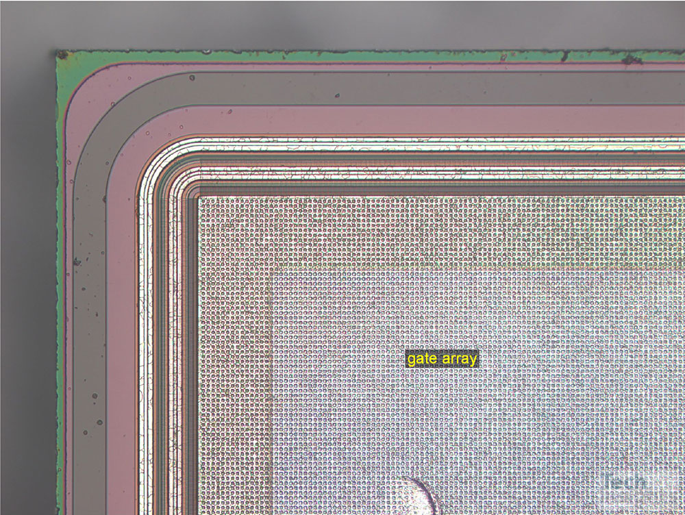
Figure 1 SCT3022ALGC11 SiC Power FET Die Corner
The layout of a single transistor cell of the SCT3022ALGC11 die at the polysilicon level can be seen in Figure 2. The square cell is comprised of a central body contact, surrounded by a dummy source trench gate. The active silicon region further surrounds the source trench. The active trench gate poly runs around the edge of each cell and is shared with adjacent cells. These active poly gates are connected electrically to the gate stringer at the edge of the array, shown in Figure 1. The transistor cell region was chosen for the process flow emulation since it represents the heart of the device.
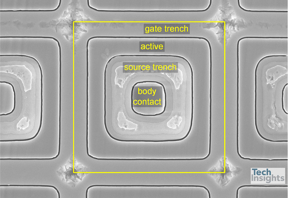
Figure 2 SCT3022ALGC11 Transistor Cell at Polysilicon – Plan-View SEM
Figure 3 shows a cross-sectional SEM image through the middle of a square transistor cell. The central body contact is connected directly to the top aluminum source metal. A source/body contact region is located adjacent to the source trenches, which is also connected to the source metal. The active gate trenches are located around the edge of the cell, as discussed for Figure 2, above.
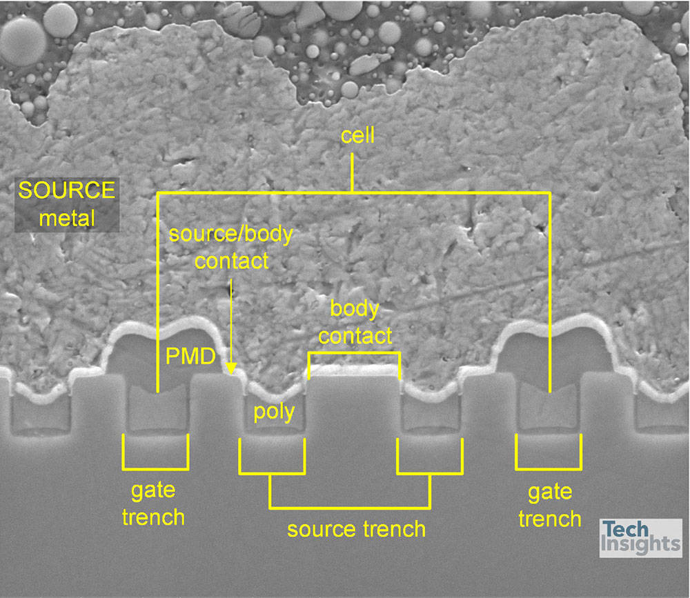
Figure 3 SCT3022ALGC11 Transistor Cell - Cross-Section SEM
Other salient features require more advanced analytical techniques. SCM is a scanning probe technique that enables delineation of the doped regions of a semiconductor structure. Figure 4 presents a cross-sectional phase-contrast SCM image through the middle of the transistor cells, centered on an active transistor trench gate. The phase-contrast SCM is sensitive to the dopant type, with P-type materials giving a positive (blue-purple) response and N-type materials giving a negative (yellow) response. The SCM shows active trench gates are formed with N-type polysilicon, and that an N+ source region is located adjacent to both sides of the trench gate. The P+ body region appears to extend around the bottom of the dummy source trenches and forms the vertical channel region on each side of the active gates. These doped regions will have been formed using dopant implant processes.
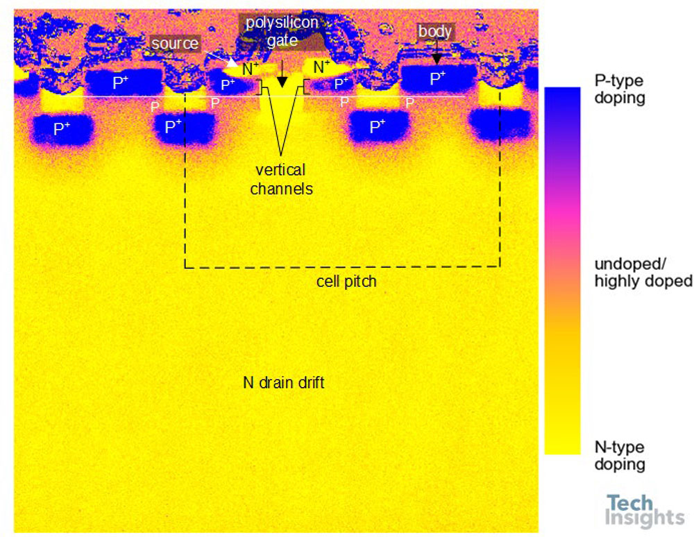
Figure 4 SCT3022ALGC11 Transistors Cell - Cross-Section SCM
TechInsights analysts interpreted the structural, materials and dopant analysis described above to build a model of the steps taken during the device process flow. The data can then be used in conjunction with the the Synopsis Sentaurus Process Explorer to emulate the process flow. Specifically, the detailed results of our reverse engineering were used to tabulate the likely process steps used in the fabrication of the SCT3022ALGC11 die. Estimated mask layouts were generated in GDSII format, based on inspection of the plan-view imaging for each layer of the device. Figure 5 presents the final structure of the transistor cell region resulting from the process emulation. A video illustrating the process steps leading up to this final structure is presented in Figure 6.
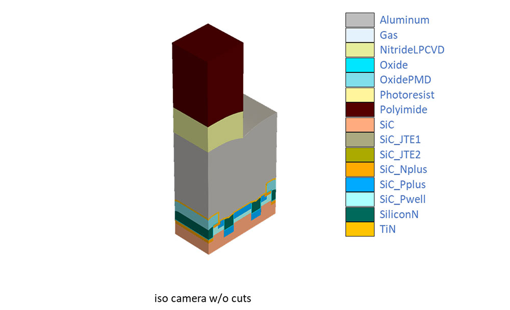
Figure 5 SCT3022ALGC11 Process Emulation Final Structure
Figure 6 SCT3022ALGC11 Synopsis Process Explorer Emulation
Process flow analysis is a value-add process reverse engineering service that delivers greater insights through interpretation of the structural information provided by plan-view and cross-sectional analysis of the device’s structure. TechInsights is now offering this service to subscription clients across several technology verticals, including Power Semiconductor, Image Sensor, Memory, and Logic.