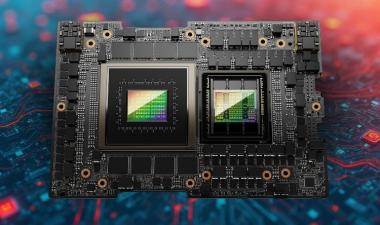
Samsung K9AHGD8J0C 133L 512 Gb TLC 3D NAND Memory Floorplan Analysis
Share This Post
Analysis of the floorplan design used in the SAMSUNG K9AHGD8J0C (V9 PRIME Die) 133L 512 Gb TLC 3D NAND and includes an executive summary and supporting image sets optical, X-ray, SEM cross sectional, and SEM bevel imaging sets. Process node and foundry identification, critical dimensions, memory and periphery functional block summaries and die/package cost analysis are provided.


