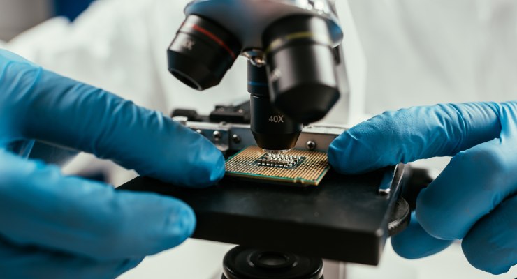
KIOXIA FYU6_1T 218L 1 Tb TLC 3D NAND Process Analysis

Discover the KIOXIA/WDC FYU6_1T (BiCS8) 218-layer TLC 3D NAND, featuring 35% higher cell current, 60% faster NAND I/O, and a 50% boost in bit density, thanks to advanced CBA and OPS technologies.
The report contents feature a detailed look at the KIOXIA/WDC FYU6_1T (BiCS8) 218-layer TLC 1024 Gb 3D NAND flash memory. This eight-generation 3D flash memory based on the bit cost scalable flash technology (BiCS8) is the first generation of KIOXIA/WDC 3D NAND to implement CMOS directly bonded to array (CBA) and On Pitch SGD (OPS) technology. By applying CBA technology to BiCS8, device performance achieved 35 percent higher cell current than conventional technology. Its high-speed NAND I/O at over 3.2Gb/s is a 60% improvement over the previous generation. OPS improved lateral scaling, with the elimination of dummy VC (instead of 24 rows of active/dummy VC, only 20 rows of active VC are used), resulting in y-axis (BL direction) packing by 16.7%. Bit density increase by more than 50 percent, resulting in highest bit density among 2XX-Layers TLC 3D NAND.


