Availability
Published
Product Code
DFR-1903-801
Product Item Code
SAM-9820
Device Manufacturer
Samsung
Device Type
Applications Processor
Subscription
Compute
Channel
Logic - Digital Floorplan (IP)
Logic - Digital Floorplan
Samsung Exynos Octa 9820 Samsung 8LPP FinFET Process Digital Floorplan Analysis
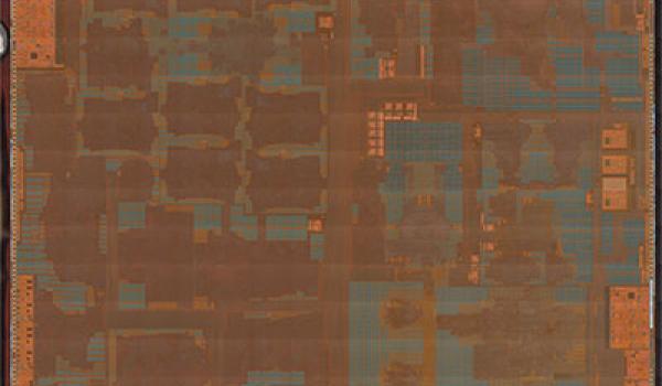
This report presents a Digital Floorplan Analysis of the S5E9820A01 die found inside the Samsung Exynos Octa 9820 application processor. The Exynos Octa 9820 processor was extracted from the Samsung Galaxy S10+ (model SM-G975F).
This report contains the following detailed information:
This report contains the following detailed information:
- Selected teardown photographs, package photographs, package X-rays, die markings, and die photographs
- Scanning electron microscopy (SEM) plan-view micrographs showing the layout of the die at the levels including fin/STI, gate, contacts, and minimum pitch metals
- Measurements of horizontal dimensions of some of the major layout features, particularly the pitch and track height of standard cells
- Plan-view optical micrograph of the die delayered to the metal gate level
- Identification of major functional blocks on a gate level die photograph
- Table of functional block sizes and percentage die utilization
- High-resolution top metal and gate level die photographs delivered in the CircuitVision software
![]()
The Authoritative Information Platform to the Semiconductor Industry.
