Latest Blogs and Commentary
LiDAR 101 – Solid-State and Mechanical LiDARs
February 19, 2021 Automotive Technology LiDAR 101 – Solid-State and Mechanical LiDARs 2020 has been an exciting year for LiDAR manufacturers. Five LiDAR companies (Velodyne Inc, Luminar Technologies Inc, Innoviz Technologies Ltd, Aeva Inc, and Ouster
Samsung 12Gb D1z LPDDR5 with EUV Lithography Applied
February 17, 2021 NAND & DRAM Memory Technology Download the brief Samsung 12Gb D1z LPDDR5 with EUV Lithography Applied After months of waiting, we have seen Samsung Electronics’ applied Extreme Ultraviolet (EUV) lithography technology for D1z DRAM
三星EUV微影製程D1z記憶體揭密
March 15, 2021 Jeongdong Choe,TechInsights 三星EUV微影製程D1z記憶體揭密 經過幾個⽉的漫⻑等待之後,三星電⼦(Samsung Electronics)採⽤極紫外光(EUV)微影製 程的D1z DRAM終於量產了! 三星電⼦在今年稍早發表了號稱業界⾸創,同時分別採⽤氟化氬浸潤式微影(ArF-i)製程與 EUV微影技術的D1z DRAM,⽽TechInsights很興奮地宣佈,我們針對三星最新/最先進 D1z DRAM的拆解分析有⼀些「新發現」
Samsung Galaxy S21 – rival 5 nm solutions, new design wins, and LPDDR5 with 1z EUV?
February 02, 2021 Teardown Disruptive Technology Samsung Galaxy S21 – rival 5 nm solutions, new design wins, and LPDDR5 with 1z EUV? Right from the release announcement, it seemed the Samsung Galaxy S21 flagship phone was going to be a little bit
A Recap of Samsung’s 108MP Image Sensors - Image Sensor TechStream Blog
February 02, 2021 Ziad Shukri A Recap of Samsung’s 108MP Image Sensors In 2019, Samsung introduced the first 108MP image sensor for mobile applications – the S5KHMX with ISOCELL Plus® technology. We first confirmed its use in the rear (wide) cam of
TechInsights Cracks Open the STMicroelectronics MasterGaN2 - Power TechStream Blog
February 02, 2021 Sinjin Dixon-Warren TechInsights Cracks Open the STMicroelectronics MasterGaN2 TechInsights recently completed a full analysis of the STMicroelectronics MasterGaN1. We found that the device contained two identical GaN Systems dies
Intel Shows Early Ponte Vecchio Part - Logic TechStream Blog
February 01, 2021 Dick James Intel Shows Early Ponte Vecchio Part Occasionally we will see something in the media that we think worth commenting on, and post as an “In Case You Missed It” (ICYMI) blog. In this case it was a Twitter post by Intel’s
Supporting IP strategy in the semiconductor industry
Supporting IP strategy in the semiconductor industry Growing complexity of the chip market has made it harder than ever for intellectual property owners to monitor developments, making reverse engineering a crucial process The breadth of reverse
HiSilicon’s move towards an antenna to modem solution - Mobile RF TechStream Blog
January 12, 2021 John Sullivan HiSilicon’s move towards an antenna to modem solution HiSilicon provides the RF transceiver and mobile SoC for Huawei’s mobile handsets but the RF front end has traditionally been sourced from the usual front end
Intel Launches 2nd-Gen 3D XPoint Memory, Discusses at IEDM - Memory TechStream Blog
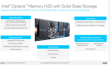
December 28, 2020 Dick James Intel Launches 2nd-Gen 3D XPoint Memory, Discusses at IEDM On Dec 16th Intel held a " Memory & Storage Moment"" where they announced five new memory and storage products; two Optane™ SSDs, one for data centers, and one
Toshiba Integrated Diode into SiC MOSFET - Power TechStream Blog
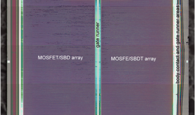
December 21, 2020 Stephen Russell Toshiba Integrated Diode into SiC MOSFET Every silicon carbide (SiC) manufacturer seemingly has their own approach to FET fabrication. Be it planar, trench, JFET, etc. there is no dominant design throughout the
Analysis of Apple M1 is Happening – and, Thermal Imaging?
Dick James, Fellow Emeritus Dick James is an almost 50-year veteran of the semiconductor industry, working in the process development, design, manufacturing, packaging and reverse engineering of semiconductor devices. Dick is a regular contributor to
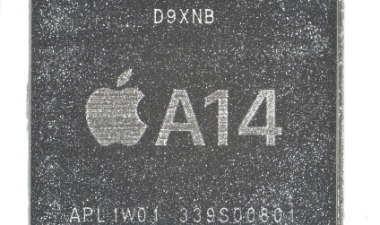
Two new Apple SoCs, two market events: Apple A14 and M1
Available Logic Subscriptions > Process & Advanced Packaging > Process Flows > Transistor Characterization > SoC Design Analysis > Digital Floorplan Analysis > Analytics - Digital Floorplan > Standard Cell GDS Library Analysis > Transistor
Teardown: Velodyne Lidar Puck VLP-16 sensor (Electronics360)
A deep dive into the major components used in the light detection and ranging technology. Posted in Electronics360.
3D flash memory, 176 layers!
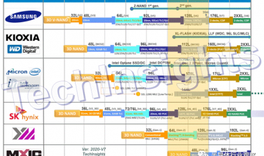
So far, NAND Flash has shown a white-hot stage. Not long ago, storage vendors were still "seeing the scenery on the high platform of flash memory" with 128 layers.
Wireless Charging Speeds Up - Teardown TechStream Blog
Stacy Wegner, Senior Technology Analyst Stacy Wegner is the Senior Technology Analyst of TechInsights’ Teardown division, responsible for ensuring the highly technical data produced by our analysts is transformed into consumable competitive
Pagination
- Previous page
- Page 54
- Next page


