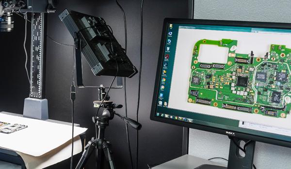
This report contains the following detailed information:
- Selected teardown photographs, package photographs, package X-rays, die markings, and die photographs
- SEM cross-sectional micrographs of the general structure of the die dielectric materials, major features, and transistors
- Measurements of vertical and horizontal dimensions of major microstructural features
- Transmission electron microscopy (TEM) cross-sectional micrographs of the transistors and the gate oxide
- TEM-based energy dispersive spectroscopy (TEM-EDS) analysis of the dielectrics, metals, and transistors


