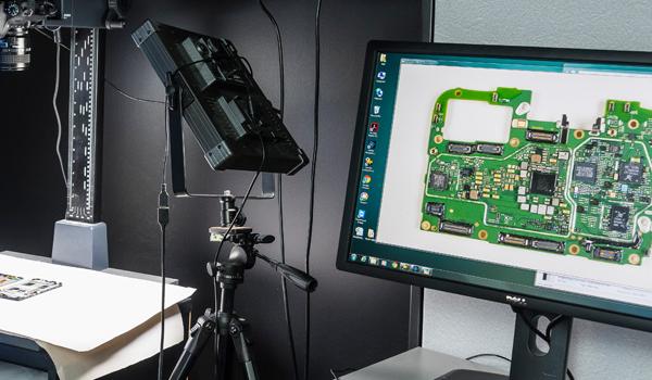
This report contains the following detailed information:
- Selected downstream and teardown photographs
- Package photographs, package X-ray, die markings, and die features
- Die utilization analysis, including an annotated gate level die photograph and functional block measurements
- Selected layout feature analysis including metal, via, and gate structures, and memory cell layout
- Scanning electron microscopy (SEM) and transmission electron microscopy (TEM) analyses of the dielectrics, metals, vias and contacts, transistors, isolation, and major structural features
- High-angle annular dark field (HAADF) scanning transmission electron microscopy (STEM) analyses of the transistor gate, gate dielectric, and S/D material
- Critical dimensions of the die features
- TEM-based energy dispersive spectroscopy (TEM-EDS) and electron energy loss spectroscopy (EELS) analyses of the dielectrics, metals, and transistors
- Scanning capacitance microscopy (SCM) and secondary ion mass spectrometry (SIMS) analyses of the wells and substrate


