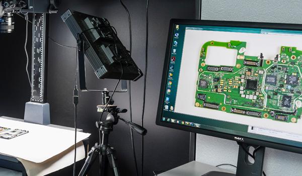
The Advanced Memory Essentials (AME) deliverable for PCM chips comprises a concise analyst’s summary document highlighting observed critical dimensions and salient features supported by the following image folders:
- Downstream product teardown
- Package X-rays, top metal and poly die photographs, non-invasive optical photos of die features
- SEM bevel through the logic region and PCM
- SEM cross section of the general device structure, BEOL (metals, dielectrics) and FEOL structures
- One (or two) TEM cross sections, orthogonal to the word (and bit) lines showing the PCM array cells, lower metals and dielectrics, transistor gates, isolation, and other FEOL features
The results of TEM-EDS analyses are included in the AME summary document. The AME deliverable provides timely competitive benchmarking information and enables cost-effective tracking of technical innovation across a breadth of competitors


