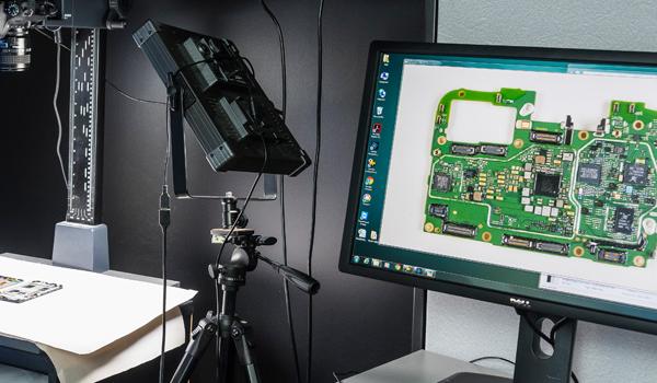
The Advanced Memory Essentials (AME) deliverable for NAND Flash chips comprises a concise analyst’s summary document highlighting observed critical dimensions and salient features supported by the following image folders:
- Downstream product teardown
- Package X-rays, top metal and poly die photographs, non-invasive optical photos of die features
- SEM bevel through the logic region and NAND flash
- SEM cross section of the general device structure, BEOL (metals, dielectrics) and FEOL structures
- One or Two TEM cross sections, orthogonal to the word and/or bit lines, showing the NAND flash array cells, the lower metals and dielectrics, transistor gates, isolation, and other FEOL features
- TEM bevel through the NAND flash
The results of TEM-EDS analyses are included in the AME summary document. The AME deliverable provides timely competitive benchmarking information and enables cost-effective tracking of technical innovation across a breadth of competitors.


