![]()
Sustainability Solutions
Frequently Asked Questions: Semiconductor Manufacturing and Carbon Emissions
The demand for increasingly powerful and fast semiconductor technology continues to increase across the globe, but so does recognition that semiconductor manufacturing can have a negative impact on the environment. With the climate crisis intensifying, the semiconductor industry faces having to both design greener processes and technologies to reduce carbon emissions while simultaneously producing more powerful semiconductors. This challenge has the industry increasingly focused on figuring out how to reduce carbon emissions from existing manufacturing facilities and also designing future sustainable chip manufacturing fabs that have a smaller carbon footprint.

A: The semiconductor industry plays a crucial role in modern technology, but its growth also contributes to rising carbon emissions. Addressing this issue is essential for mitigating climate change.
A: The industry faces a two-part challenge:
- Developing greener processes and technologies to create more powerful semiconductors with lower environmental impact.
- Reducing emissions from existing manufacturing facilities.
A: Scope 1 emissions come directly from a facility's activities, such as burning natural gas to on-site to heat a building. Scope 2 emissions are indirect emissions from purchased electricity. Understanding these categories helps identify areas for emission reduction.
A: Scope 3 emissions are those that result of activities from assets not owned or controlled by the reporting organization, but that the organization indirectly affects in its value chain. TechInsights will initially focus on Scope 3 emissions from Category 1: Purchased Good and Services and Upstream Transportation.
A: This module is a valuable tool for calculating and comparing carbon emissions from IC die and silicon wafer manufacturing. It covers a range of processes and technologies, allowing users to assess and compare the environmental impact of equipment, processes, and manufacturing steps for Logic, DRAM, and NAND for leading 300mm wafers, as well as legacy processes on 200mm wafers and below.
A: The key emissions elements to be addressed include:
- Breakdown of Scope 1, 2, and 3 emissions from die manufacturing.
- Comparison of carbon emissions based on:
- Purchased electricity
- On-site fossil fuel usage
- Process gas usage and abatement efforts, including data on PFAS chemicals
- Water consumption
- Historical and future emission scenarios for informed decision-making
A: This model is designed to support various players in the semiconductor value chain:
- Foundries, Fabless vendors, and IDMs can use it to optimize design choices and evaluate investments in new equipment for lower emissions.
- Capital equipment vendors can benchmark their tools against competitors to demonstrate environmental benefits.
- Product manufacturers can use the module for life cycle analysis and emissions reporting.
- Government can use it to analyze the impacts and benefits of manufacturing onshoring, as well as having unbiased data that can triangulate reported values from organizations across the value chain.
A: The Manufacturing Carbon Module is based on TechInsights’ ongoing evidence-based analysis conducted by our Technical Analysis engineering teams. Molule outputs are validated using public information, including U.S. EPA summary sheets, company data from semiconductor manufacturers, acquired data sets, and information from environmental data sources.
A: The TechInsights Manufacturing Carbon Module database is continuously updated as more technology nodes come online. The module now covers more than 370 fabs worldwide and more than 950 processes from 87 semiconductor manufacturers, from 2015-2035. This allows users to compare historical results to current and future scenarios.
A: All customer queries and activities within the Platform remain secure and are not accessible to any other accounts. The only exception would be a query that a customer created, saved, and then chose to share with other users within their organization.
A: Users are able to review, compare, and benchmark how changing processes and process steps affect carbon footprints and emissions over time. This information is critical for vendors across the semiconductor value chain to benchmark, analyze, and report carbon impact at the micro and macro level. The module allows users to stay ahead of understand carbon footprint trends, get insight into equipment and process choices being made by the competition, and make informed decisions for long-term environmental gains and contribute to a healthier planet. Customers also use this tool to satisfy product carbon footprint requests from their customers during the bidding process.
Technology covered includes:
- Logic (3000nm to 3A)
- DRAM (150nm to 0B/1ε)
- 2DNAND (12x to 1z)
- 3DNAND (24L to 1024L)
- Power (3,000nm to 90nm)
- High-bandwidth Memory
- Interposers
A: The TechInsights Manufacturing Carbon Module provides evidence-based carbon emissions data for semiconductor fabs worldwide, including those forecast to come online through 2035 and includes known fabs under construction.
By using the TechInsights Manufacturing Carbon Module, companies can gain valuable insights and contribute to a brighter future for sustainable chip manufacturing.
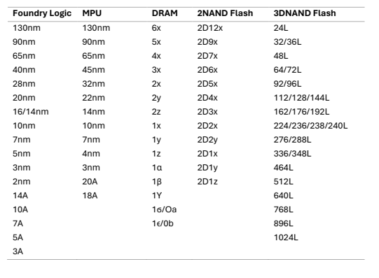
Node is a term used to define a device technology generation and has significant impact on the equipment toolset and materials required for semiconductor manufacturing. In the early years of the industry node meant the minimum half-pitch of the smallest patterned feature on the chip, but in recent years the term now refers to a greater number of transistors per silicon area.
Logic chips have nodes expressed in nanometers (i.e., “28N” or “3N”) with a transition to angstroms (i.e., “18A” or “14A”) on the horizon. The most advanced fabs use a variety of lithography technologies to do patterning at different minimum pitches: Extreme Ultraviolet (EUV) only for the tightest pitches near the transistors, Deep Ultraviolet (DUV) for on-chip interconnects, and I-line for bond-pads and package-level interconnects.
Memory has evolved from 2D to 3D device architectures, led by non-volatile 3DNAND chips. 3DNAND memory is characterized by the number of horizontal layers stacked. DRAM may eventually transition to 3D, yet while still in 2D the node is characterized by a vague relative nanometer term (e.g., “2x” or “2y” see Table below).
In this model, foundry logic is used as the nodes for equipment definitions, which is then aligned to the other products’ nodes. Memory node alignments are by the year. They are expected to be introduced into high-volume manufacturing (HVM). For example, 276-layer (276L) 3DNAND uses the same equipment as 7nm Logic.
Node Equivalents in the Model
Earth Day 2025: A Progress Report on Sustainable Semiconductor Manufacturing
Can the chip industry scale innovation and sustainability? Discover the current state of green tech in one of the world’s most energy-intensive sectors.

Stay ahead of the curve with TechInsights Tariff Watch, your go-to resource for timely and in-depth analysis on the shifting landscape of tariffs and their impact on the tech industry.

TechInsights Appoints Dan Kim as Chief Strategy Officer
TechInsights has announced the appointment of Dan Kim as its new chief strategy officer, effective April 21, 2025. In this new role, Kim will lead TechInsights’ strategy and engagement with corporate and government customers across the Americas, Europe, and Asia.
The authoritative information platform to the semiconductor industry.
Discover why TechInsights stands as the semiconductor industry's most trusted source for actionable, in-depth intelligence.